DVM - Design Verification Module
DVM - Design Verification Module
|
The pulse input source can be configured to pulse the input voltage between two or three voltages. This source is used in the PulseLine() Test Objective.
Other similar sources include:
In this Topic Hide
Model Name |
Pulse Input Source |
|
Simulator |
|
This device is compatible with both the SIMetrix and SIMPLIS simulators. |
Parts Selector |
DVM ▶Source ▶Input Source |
|
Symbol Library |
None - the symbol is automatically generated when placed or edited. |
|
Model File |
SIMPLIS_DVM_ADVANCED.lb |
|
| Subcircuit Name | SIMPLIS_DVM_ADVANCED_SOURCE_PULSE | |
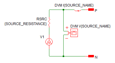
| Schematic |
|
|
The following table explains the relevant parameters.
| Parameter Name | Default | Data Type | Range | Units | Parameter Description |
FALL_TIME |
50u | Real | min: 0 | s | The fall time of the source |
FINAL_VOLTAGE |
12 | Real | V | The final voltage of the source | |
PULSE_VOLTAGE |
9 | Real | V | The pulse voltage of the source | |
PULSE_WIDTH |
200u | Real | min: 0 | s | The time which the source voltage is the PULSE_VOLTAGE |
RISE_TIME |
100u | Real | min: 0 | s | The pulse rise time in seconds |
SOURCE_NAME |
SRC | String | n/a | n/a | Name of the DVM source. This name cannot contain spaces. |
SOURCE_RESISTANCE |
0.4 | Real | min:0 | Ω | Sets the source resistance of the source |
START_VOLTAGE |
5 | Real | V | The starting voltage for the source | |
TIME_DELAY |
10u | Real | min: 0 | s | The time delay before the pulse initiates |
To set any managed DVM source to a Pulse Input Source subcircuit, place a Pulse testplan entry in the Source column.
The Pulse() testplan entry has the following syntax with the arguments explained in the table below.
Pulse(REF, START_VOLTAGE, PULSE_VOLTAGE,
FINAL_VOLTAGE)
Pulse(REF, START_VOLTAGE, PULSE_VOLTAGE, FINAL_VOLTAGE,
OPTIONAL_PARAMETER_STRING)
where:
| Argument | Range | Description |
REF |
n/a |
The actual reference designator of the DVM source or the more generic syntax of INPUT:n where n is an integer indicating a position in the list of managed DVM sources. |
START_VOLTAGE |
min: 0 |
The starting voltage for the source. This can be a numeric value or a symbolic value, such as a percentage of the nominal source voltage. |
PULSE_VOLTAGE |
min: 0 |
The pulse voltage for the source. This can be a numeric value or a symbolic value, such as a percentage of the nominal source voltage. |
FINAL_VOLTAGE |
min: 0 |
The final voltage for the source. This can be a numeric value or a symbolic value, such as a percentage of the nominal source voltage. |
OPTIONAL_PARAMETER_STRING |
n/a |
Parameter string with a combination of one or more timing parameters:
|
* If more than one parameter is specified, join the parameter key-value pairs with a space, as shown in the example below. The order of the parameter names does not matter.
The timing for the Pulse Source is determined by the following parameters.
Timing parameters can be assigned using the optional parameter string as shown in the following examples.
This example shows a symmetric pulse with equal rise and fall times. The final voltage is the same as the starting voltage.
| *?@ Source | ||||
|---|---|---|---|---|
| Pulse(INPUT:1, 1, 5, 1, TIME_DELAY=25u RISE_TIME=25u PULSE_WIDTH=100u FALL_TIME=25u) | ||||
The results of this testplan entry are shown below:
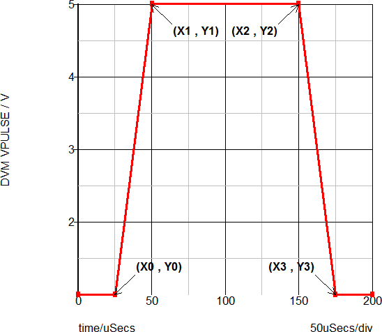
| Annotation | Value |
| X0 | TIME_DELAY |
| X1 | TIME_DELAY + RISE_TIME |
| X2 | TIME_DELAY + RISE_TIME + PULSE_WIDTH |
| X3 | TIME_DELAY + RISE_TIME + PULSE_WIDTH + FALL_TIME |
| Y0 | START_VOLTAGE |
| Y1 | PULSE_VOLTAGE |
| Y2 | PULSE_VOLTAGE |
| Y3 | FINAL_VOLTAGE |
The following example sets the first DVM managed source to a Pulse Voltage Source, with a starting voltage of 1V, a pulse voltage of 5V and a final voltage of 4.5V. Note the rise and fall times are not the same and the pulse does not have to return to the starting voltage value.
| *?@ Source | ||||
|---|---|---|---|---|
| Pulse(INPUT:1, 1, 5, 4.5, TIME_DELAY=25u RISE_TIME=25u PULSE_WIDTH=75u FALL_TIME=50u) | ||||
The results of this testplan entry are shown below:
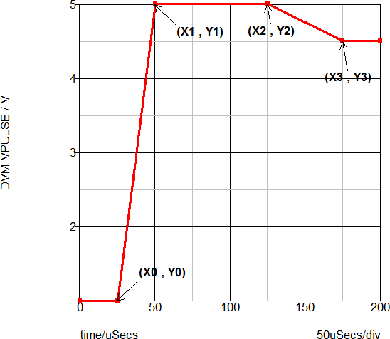
| Annotation | Value |
| X0 | TIME_DELAY |
| X1 | TIME_DELAY + RISE_TIME |
| X2 | TIME_DELAY + RISE_TIME + PULSE_WIDTH |
| X3 | TIME_DELAY + RISE_TIME + PULSE_WIDTH + FALL_TIME |
| Y0 | START_VOLTAGE |
| Y1 | PULSE_VOLTAGE |
| Y2 | PULSE_VOLTAGE |
| Y3 | FINAL_VOLTAGE |
© 2015 simplistechnologies.com | All Rights Reserved