Verilog-HDL Interface (VSXA)
In this topic:
Overview
The VSXA device provides digital functionality defined by a Verilog-HDL definition. The connections to the VSXA device map directly to input and output ports defined within the Verilog-HDL module and may be connected to analog or digital SIMetrix components or other VSXA devices.
The Verilog-HDL simulation is performed by an external Verilog simulator and at least one such simulator is supplied with SIMetrix and is pre-installed with no additional setup or configuration required. Communication between the external Verilog-HDL simulator is achieved through the VPI programming interface and in principle this can allow any VPI compliant Verilog-HDL simulator to be used for this purpose.
This section describes details of the VSXA device. For more general information about using the Verilog-HDL feature, refer to Chapter 13 in the User's Manual.
Netlist
Uxxxx nodes modelname
| nodes | Nodes connecting to Verilog device. Nodes that appear here map directly to the port connections in the top level module in the Verilog file defined in the associated .MODEL statement. If the Verilog definition contains vector connections, the sizes of those connections may be defined using the PORTSIZES model parameter. See below for details. |
| modelname | Name of model. Used to reference .MODEL statement |
Model Syntax
MODEL modelname vsxa parameters
| Name | Description | Units | Default |
| LOAD | Path to file name of Verilog definition. | n/a | Compulsory |
| IN_LOW | Input analog low threshold voltage. A logic zero will be detected when the analog voltage drops below this threshold | V | 2.2 |
| IN_HIGH | Input analog high threshold voltage. A logic one will be detected when the analog voltage rises above this threshold | V | 2.3 |
| OUT_LOW | Output voltage for a logic zero | V | 0 |
| OUT_HIGH | Output voltage for a logic one | V | 5 |
| T_RISE | Output rise time | sec | 100p |
| T_FALL | Output fall time | sec | 100p |
| IN_RES | Input resistance | Ohms | 1e12 |
| OUT_RES | Output resistance for logic zero and logic one states | Ohms | 100 |
| OUT_RES_HIZ | Output resistance for the high impedance state | Ohms | 1e12 |
| TIME_TOL | Input threshold time tolerance. This parameter works in the same way as the TIME_TOL parameter defined for the A-D Interface bridge used in the built-in digital simulator. This is described in Time Step Control - TIME_TOL parameter | sec | 100p |
| DISABLE_INTERNAL_VECTORS | VSXA instances that are connected to each other but not to any other SIMetrix device still generate digital vectors to allow plotting of those nodes. Setting this parameter to 1 disables this | 0 (false) | |
| DISABLE_ MODULE_ CACHE | No cache data will be created for this model. | 0 (false) | |
| PORTSIZES | Array of values defining the size of each port. If any of the Verilog ports are vectors, SIMetrix needs to know their size. If this parameter is not specified, it will assume they are the size defined in the Verilog module. If any is actually smaller, this needs to be defined in this parameter. This is a vector value with one value for each port. So if there are three ports, PORTSIZES would be set like this for example: PORTSIZES=[2,3,5] which would set the first port to size 2, the second to size 3 and the last to size 5 | see description | |
| PORTINIT | Initial state for input ports if dc solution lies between in_low and in_high. This is a vector value with one value for each input port. So if there are two input ports, PORTINIT would be set like this for example: PORTINIT=[1,1] which would set both ports to a logic one indicating if the analog input lies between the defined thresholds. If a PORTINIT value is set to 2, the port will be set to the UNKNOWN state. Note that vector ports are treated as one for this parameter. | 0 |
Analog Input Interface
Any port in the Verilog definition that is defined as an input will be treated by the analog simulator as a VSXA input connection. This has the following characteristics:
- Input resistance equal to the value of the in_res model parameter.
- Detects a logic one when the input signal rises above a voltage equal to the in_high model parameter.
- Detects a logic low when the input signal drops below a voltage equal to the in_low model parameter.
- When the input voltage is between the in_low and in_high values, the signal detected will be the most recent value detected, that is it will hold its value like a schmitt trigger. For DC and t=0 the value will be that defined by the PORTINIT parameter. This is logic zero by default. A PORTINIT value of 1 will set this to logic one and any other value will set it to an unknown state.
- The analog system will only send an UNKNOWN state to a Verilog input if the DC voltage lies between the thresholds and the corresponding PORTINIT value is other than 0 or 1. Once an input has acquired a logic zero or logic one state, it will thereafter behave as a schmitt trigger.
Analog Output Interface
Any port in the Verilog definition that is defined as an output will be treated by the analog simulator as a VSXA output connection. This is modelled as shown in the following diagram:
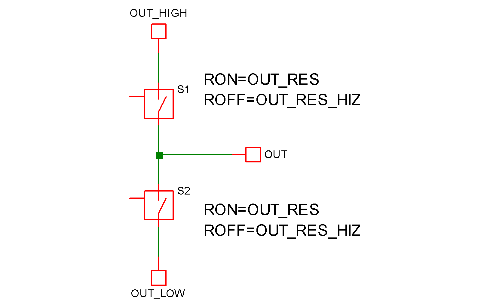
Each switch has an on state resistance of OUT_RES and an off state resistance of OUT_RES_HIZ. In the logic one state, S1 is on, in the logic zero state S2 on, while in the high-impedance state, neither switch is on. When transitioning from one state to another state, each switch's resistance changes linearly to the new state's value in the time determined by the parameters T_RISE and T_FALL.
Important: A VSXA output that is only connected to VSXA inputs is implemented entirely within the Verilog domain and are not connected to the analog simulator.
Data Vector Output
Voltage Data
Connections between VSXA devices and any other SIMetrix device (including non-Verilog digital devices) are analog nodes in every way and will generate voltage data vectors in the usual way.
Connections between VSXA devices and other VSXA devices that do not connect to anything else and do not connect more than one Verilog module output port are implemented entirely within the Verilog simulator domain and do not interface to the analog simulator. For such connections, digital data vectors are created. These transition between the values OUT_LOW and OUT_HIGH with rise and fall times equal to the timing resolution set by the VerilogResolution option setting. This defaults to 1fs.
In some situations it is possible that the overhead of creating this data could slow down the simulation. This would be the case where such internally connected signals carry high speed data that is much faster than the analog time steps. In these cases the output of this data can be disabled using the DISABLE_INTERNAL_VECTORS parameter for the VSXA device that carries the output driving port. They can also be globally disabled using the VerilogDisableInternalVectors .OPTIONS setting.
Current Data
VSXA devices generate current vectors in the normal way for all connections that connect to analog signals. These vectors are named as follows:
ref#port_nameIn the case of vector ports port_name is the name of the port appended with the index of the wire within the port. For example, with the following Verilog definition:
module adder(in1, in2, out) ;

input [3:0] in1 ;
input [3:0] in2 ;
output [3:0] out ;
the port_names for the out port would be out0, out1, out2 and out3.
Module Cache
Operation
Before starting a simulation and also when creating a symbol from a Verilog design, SIMetrix needs to gather some information about each Verilog module used in the circuit. It does this by starting a Verilog simulation then interrogating the Verilog simulator via VPI. This process can take some time if there are many Verilog modules in the circuit. To speed things up, SIMetrix caches the information obtained for future use.
The cache mechanism calculates the MD5 checksum of the Verilog file and stores this with the cached information in the cache file. When the cached information is required, SIMetrix calculates the MD5 checksum of the Verilog file and looks to see whether there is a cache item with that MD5 value. If there is, it will use the cached data. If not it will retrieve the information via the Verilog simulator.
Location
The cache file is located at vldatapath/module-cache.sxche
Where vldatapath is a directory defined by the VlDataPath global option setting. This can be set using the Set command typed at the command line. E.g.
Set VlDataPath=path
The default value of path is:
simetrix_app_data_dir/veriloghdl
simetrix_app_data_dir is the directory where SIMetrix configuration settings are stored and defaults to C:???MATH???\backslash???MATH???Users???MATH???\backslash???MATH???login-name???MATH???\backslash???MATH???AppData???MATH???\backslash???MATH???Roaming. Refer to User's Manual/Sundry Topics/Configuration Settings/Application Data Directory for details about the Application Data path simetrix_app_data_dir.
Be aware that this file is created when a simulation is closed. This takes place when a new simulation is started, when the Reset script command is executed or when the simulator process terminates.
Limitations
The cache mechanism only looks at the contents of the Verilog file referenced. It does not take account of include files for example. However, the only information stored in the cache are the module name, names and direction of the module ports and the names, types and default values of any parameters. It would be ususual to store these items in an include file but of course this is perfectly legal.
If the top level ports or/and parameters for your Verilog design are nor defined in the main file but in an include file, then you should either redesign the Verilog file or alternatively disable the cache for that module.
The cache can be disabled by setting the DISABLE_MODULE_CACHE model parameter. Important: the DISABLE_MODULE_CACHE parameter disables the creation of cached information; it does not disable using cached information if it already exists. This is because the cache is read before model parameters are read. You may wish to clear the cache altogether when setting this parameter. This can be done from the front end with menu .
The cache can also be globally disabled using the .OPTIONS setting VerilogDisableModuleCache.
| ◄ Mutual Inductor | NXP Compact Models ▶ |