Advanced SIMPLIS Training
Advanced SIMPLIS Training
|
To download the examples for Module 7, click Module_7_Examples.zip
In this Topic Hide
Using the methodology outlined in Module 6, you will create a model for a MOSFET driver that will support the model requirements below. During this process, you will learn:
How to use a PWL resistor to model the output characteristics of a driver MOSFET.
The value of parameterizing your simulation models so that it may be used as a general purpose modeling blocks in future projects.
The value of characterizing the simulation performance each SIMPLIS modeling block.
The importance of creating testbenches for each modeling block.
The MOSFET Driver modeling block should:
Model the losses of a single MOSFET/Driver combination including both conduction and switching losses during turn-ON and turn-OFF.
Parameterize the MOSFET Driver model so that it may be used as a general purpose modeling block.
Isolate the PWM driver input signal from the gate drive source and sink currents.
Provide a parameterized asynchronous delay to the PWM input signal, allowing different values for the driver turn-ON delay and turn-OFF delay under no-load conditions.
The design procedure for this model is broken into five steps.
The purpose of a development testbench is to create a test environment in which to efficiently develop a subcircuit simulation model. Eventually, our driver model will be contained within a subcircuit as part of a hierarchical system model. In Module 6, you began developing our Load Model immediately as a subcircuit model. However, with this testbench we initially start out our development with our driver model in the same flat schematic as our testbench. For relatively small but operationally complex circuits, this approach can have the advantage of allowing the modeler to see the model being developed at the same hierarchical level as the circuitry driving its input and being driven by its output.
During the development of a single modeling block, the timing of when one moves from a flat development testbench to a hierarchical testbench is a judgement call best made by the modeler. However, the end product of each functional sub block model development should always be a hierarchical subcircuit. As a general rule, when a functional sub block model is being characterized and successfully tested against its model requirements, it should already be an appropriately parameterized hierarchical subcircuit. Very large flat schematics become extremely hard to manage and are virtually impossible for anyone but the original modeling engineer to understand. And after some time passes, even the original engineer will struggle to make sense of how the circuit works.
In order for our driver testbench to support efficient subcircuit development, the testbench simulations should
Run fast
Exercise the critical driver performance requirements
Allow incremental development of the driver model
Facilitate the creation of a subcircuit model
For this example, the Synchronous Buck example circuit from the SIMPLIS Tutorial 1.2_SIMPLIS_tutorial_buck_converter.sxsch is used as the foundation of our development testbench.

Further, in this testbench, we focus all our attention on the high side MOSFET Q1 and its driver. We will assume instantaneous switching for the low side Synchronous MOSFET represented by D1.
Next we modify this schematic to support the development of a MOSFET driver modeling block that will meet our model requirements above. The first step is to spread out the circuit to make room for our detailed driver block in the middle, as shown below.
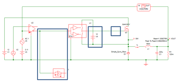
In addition to making room for the driver circuit, we also
Remove gate resistor R2 in series with the gate of Q1,
Change the value of the voltage on V4 to 12V,
Move the position of the POP Trigger schematic device to the output of the comparator U2
Change the model of D1 to User-defined with the following parameters:
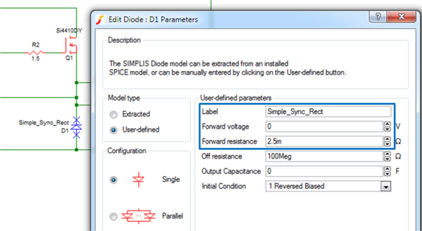
It is interesting to note that this is a very effective way to model a synchronous MOSFET where we are not interested in modeling the non-ideal switching behavior of that device. Instead, we have a very simple Sync MOSFET model that accurately models the conduction losses, but, because it switches instantaneously, produces no switching losses in either the high-side or low-side MOSFET. In effect, D1 behaves like a MOSFET with ideal gate drive waveforms and zero capacitance.
The schematic 7.1_buck_w_driver_step1.sxsch shows our progress thus far at the end of Step 1.
For accurate simulations of a switching power MOSFET, it is essential that both the MOSFET and its drive circuit be well modeled. We already know from earlier discussions in Module 1.0.4 Multi-Level Modeling that we need at least a level 2 SIMPLIS MOSFET model to model its switching voltage and current waveforms. However, this is in no way sufficient. In order to model the switching losses of Q1, we must also accurately model both the charging current and the discharging current of the driver as it charges and discharges the Gate-to-Source capacitance of the power switch Q1 during the turn-ON and turn-OFF transitions.
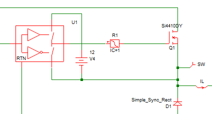
For the purposes of this example, we will assume that the output stage of the MOSFET Driver is also made up of MOSFETs QDHS and QDLS in a totem pole configuration as shown here.
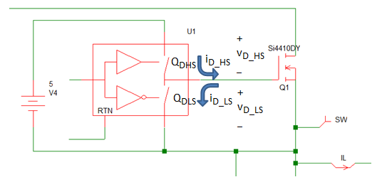
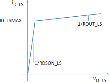
The question then becomes, how can we model the ideal switching behavior of the high side driver MOSFET QDHS and the low side driver MOSFET QDLS? In this example, we will assume that we can characterize the output drive currents iD_HS and iD_LS of the high side driver QDHS and the low side driver QDLS, respectively as shown here.
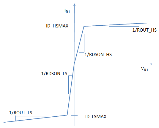
We can now complete the detailed requirements of our Driver model by saying that our driver must model the characteristics of QDHS and QDLS as shown above. In addition, we want to pass the driver model the parameters RDSON_HS, ID_HSMAX, ROUT_HS, RDSON_LS, ID_LSMAX and ROUT_LS.
In the previous two figures, we anticipate that the characteristics of QDHS and QDLS are likely different in both their respective values of RDSON as well as their maximum current capability ID_HSMAX and ID_LSMAX, respectively. An assumption that we are making is that the gate drive for both QDHS and QDLS is constant and independent of the loading of the driver output.
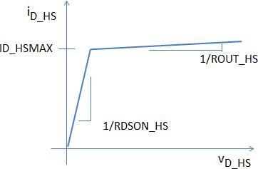
Looking at the iD_HS versus vD_HS characteristics of QDHS, the driver high side MOSFET, it is clear that this behavior can be modeled in SIMPLIS by a PWL resistor. The same is true for QDLS, the driver low side MOSFET. In fact both QDHS and QDLS can be modeled by a single PWL resistor as shown here.
The definition of this PWL resistor is illustrated in this next figure, where the behavior of QDHS is shown in the first quadrant of the piecewise linear current iR1 versus voltage vR1 plot and the behavior of QDLS is shown in the third quadrant.
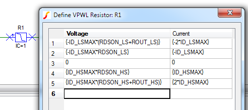
Based on the characteristics above, the PWL resistor R1 can be parameterized as shown here.
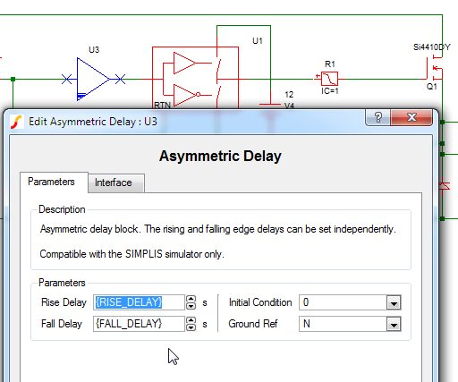
Our final model requirement that needs to be addressed is the asymmetric delay of the input signal to the driver. Here we want the rise delay and the fall delay to be parameterized independently.
After verifying that this flat driver testbench demonstrates the capability of meeting our model requirements, it is time to create a driver subcircuit with an appropriate symbol and then parameterize it as indicated above. We can then refine the model as necessary, but we want to invest the majority of our testing efforts on the model in its final subcircuit form.
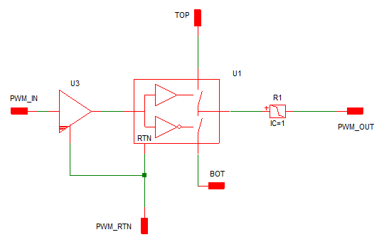
The schematic 7.2_flat_development_schematic.sxsch is the final flat schematic before converting the driver to a subcircuit. At this point, we are ready to create a subcircuit for the MOSFET Driver where its parameters are defined in the F11 window of the subcircuit.
The following subcircuit schematic 7.3_driver_subcircuit_params_in_F11_window.sxcmp shows the Driver model with both the asymmetric delay block and the PWL resistor parameterized as illustrated above.
One aspect that we have not addressed yet is the saturation resistance of the top and bottom switch in the driver block U1. When the top switch of U1 is ON, the possibility exists that the resistance of that top switch could be of a comparable resistance to the RDSON_HS parameter of the PWL resistor R1. In order to not have to worry about this possibility, we can parameterize the Saturation Resistance of the Top Switch to be a small fraction of RDSON_HS as shown here.
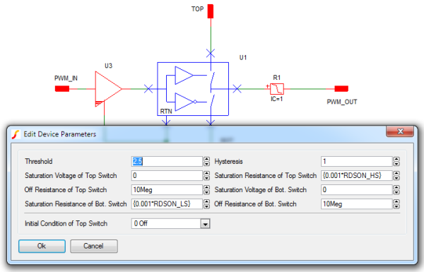
The same can be done for the Saturation Resistance of the Bot. Switch of U1. It can be made to be a small fraction of RDSON_LS.
Early in the subcircuit model development process, it makes sense to set the parameter values by using .var statements in the F11 window of the subcircuit itself as is the case with 7.3_driver_subcircuit_params_in_F11_window.sxcmp
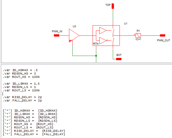
This allows the developer to focus their initial efforts on the correct parameterization of each of the elements in the subcircuit model. It also facilitates the initial verification of the subcircuit performance in the development testbench. As can be seen in this testbench 7.3_sync_buck_w_driver_no_GUI.sxsch we are using the default automatically created symbol and there is no GUI to facilitate changing the subcircuit parameter values from the symbol on the top level schematic.
However, once the functionality of the model is confirmed, it quickly becomes worthwhile to invest in adding the needed properties to the symbol allowing parameter values to be passed through the subcircuit symbol as described in Module 5. It will also be worth the modest time investment to enhance the look of the symbol if this modeling block can be reused in future projects.
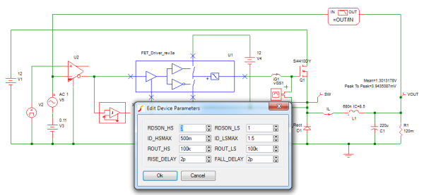
Here the schematic 7.4_sync_buck_w_parameterized_driver_w_GUI.sxsch presents a more informative symbol and a GUI dialog box for this Driver subcircuit that were created using the steps described in Module 5 on Parameterization.
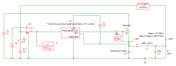
Since our ultimate objective is the evaluation of MOSFET switching losses with our Driver model, at least two testbench circuits are needed. The first is just to test the Driver model itself. The second is to test the Driver model while driving an N-channel MOSFET.
For each test bench, we will record several metrics to characterize the simulation performance of the Driver - testbench combination. After each simulation, we will record the minimum time constant of the testbench circuit as well as the number of New Topologies needed to reach steady state. As soon as the simulation is complete, we click on the menu item "Show Smallest Time Constant".
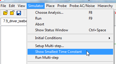
We also look in the SIMPLIS Status window and record the number of New Topologies required to reach steady state. The results of these queries are pasted underneath each testbench schematic.
In our first testbench 7.5_driver_testbench_cap_load.sxsch we test the Driver modeling block with a pure capacitive load.
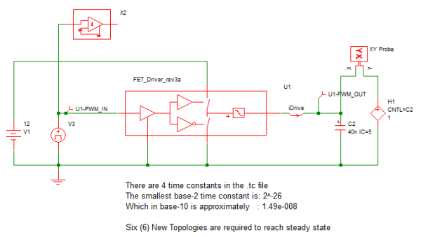
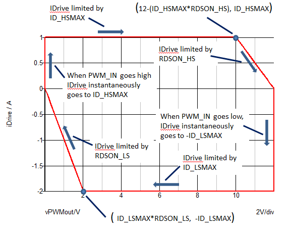
This is a very good way to make sure that the driver block is behaving as expected. As we can see, when the capacitor voltage is initially rising, it is being charged with essentially a constant current source. Once the voltage across the PWL resistor R1 inside the Driver model reaches a value of ID_HSMAX * RDSON_HS or less, then the charging current iDrive begins an exponential RC decay. The discharge current behaves in an analogous fashion.
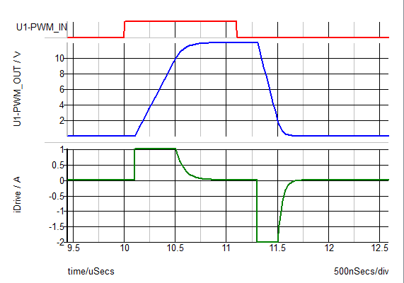
It is very easy to verify the key Drive model break points from a graph of iDrive versus vPWMout.
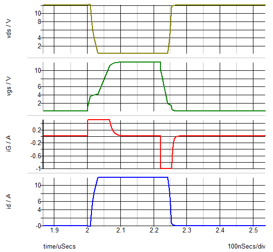
Our next two testbenches look at the performance of the combination of the Driver model and an NMOS device driving a resistive load. In the first case, 7.6_driver_testbench_Lev0_mos_load.sxsch the power switch is modeled with a Level 0 MOSFET model, which models the gate capacitance and exhibits instantaneous switching when the device turns ON or OFF.
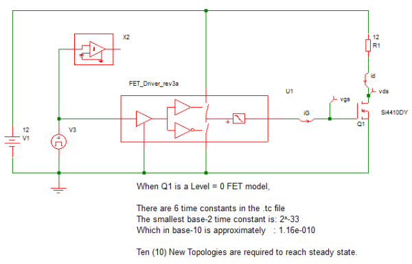
The resulting steady-state waveforms generated by 7.6_driver_testbench_Lev0_mos_load.sxsch show the instantaneous switching as well as the same charging and discharging behavior of the gate capacitance as we observed in the testbench with the pure capacitive load. The only slight difference is that at the initiation of turn ON and turn OFF, you can see the effect of the 1.55 Ohm gate resistance of the Si4410DY MOSFET.
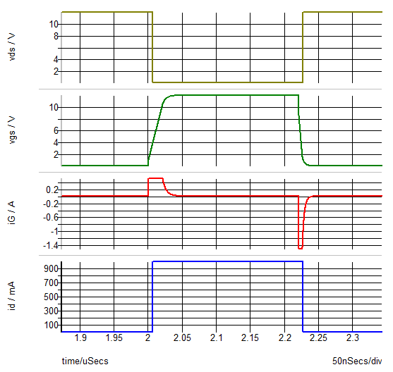
Our next testbench 7.7_driver_testbench_Lev2_mos_load.sxsch changes the MOSFET model level from 0 to 2. It is still employing a resistive load.
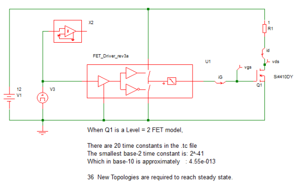
The resulting waveforms show the expected Miller effect during turn ON and turn OFF. We also note that the number of New Topologies increases significantly when we go from a Level 0 MOSFET model to Level 2. We also can see that the minimum time constant is three orders of magnitude smaller with the Level 2 model. Bear in mind that these results are for the simplified case where we are greatly simplifying the model of the synchronous MOSFET, modeled here as D1.
These results give us confidence that our Driver model is capturing the behavior that we intended and that the model construction is sound. We also have a good quantitative sense of the complexity of the driver model which will allow us to better predict what kind of simulation performance we can expect as we add this driver model into larger and more complex systems.
In the next step, we will test to see if we can use this driver model to obtain meaningful estimates of switching losses of the high side MOSFET in a synchronous buck dc-to-dc converter.
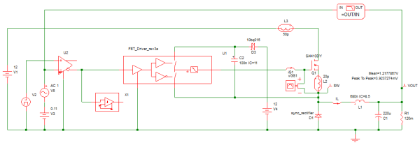
To begin, we first add a bootstrap capacitor to our circuit, replacing the dedicated source V4 in 7.3_sync_buck_w_driver_no_GUI.sxsch.
In the resulting schematic 7.8_driver_w_bootstrap_cap.sxsch the bootstrap capacitor is connected to the independent source V4, which for this example is connected set to 12V.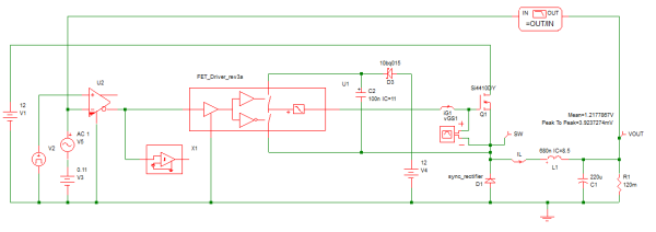
Below are the resulting steady-state waveforms of the gate voltage vGS1, gate current iG1, switch node voltage SW and the inductor current iL.
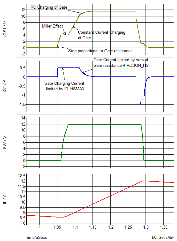
During the turn ON transition, the gate current steps up to a value of ID_HSMAX causing a small step in the gate voltage corresponding to the resulting voltage across the gate resistance of Q1, which in this example is 1.55 Ohms. Next the gate voltage reflects the fact that the input capacitance of Q1 is charged by a constant gate current equal to ID_HSMAX until the gate voltage reaches a value that allows all the inductor current iL to flow through Q1. At this point, the drain-to-source voltage begins its transition from high to low and the switch node SW transitions from low to high.
During the turn ON switching transition, assuming the gain of the transitor is reasonably high, the gate voltage plateaus at a voltage such that the rate of change of drain-to-gate voltage is equal to gate charging current divided by the nonlinear gate-to-drain capacitance.
Once the turn-ON switching transition is complete, then the gate voltage continues to be charged up to its maximum value. This rate of charge is set by IS_HSMAX until the voltage difference between the driver positive supply node and the gate capacitor decreases to the point where the charging current is then limited by the voltage drop across RDSON_HS + the gate resistance.
The gate discharge and the resulting turn OFF transition happen in an analogous fashion as shown below.
There is one interesting possible difference in the discharge waveforms. In this example, we see a second plateau on the gate voltage during turn OFF that was not present during the turn ON transition. This occurs because by the time that the gate voltage reaches the voltage corresponding to the maximum inductor current iL, the gate voltage is low enough that the discharging current is limited by the series combination of gate resistance + RDSON_LS.
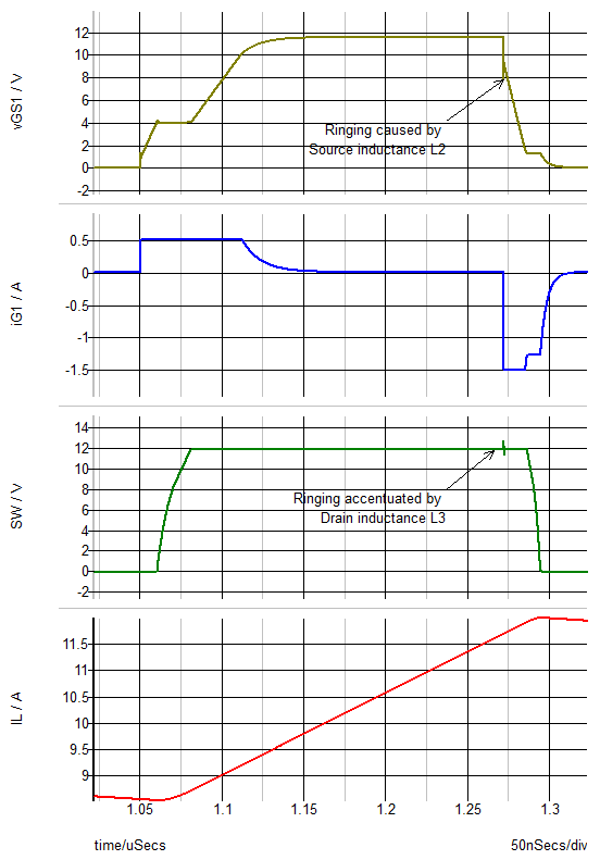
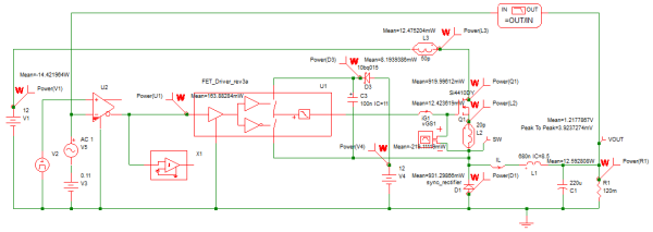
In our next example schematic 7.9_driver_w_parasitic_inductances.sxsch, we add parasitic inductance in series with the source and drain leads of Q1. These inductances can represent either package impedance or PCB layout impedance, or both.
Of these two parasitic inductances, the source inductance L2 is by far the most important. The ringing in the vGS1 and the pulse in the switch node waveform SW is caused by the source inductance L2. The Q of the ringing in the SW waveform caused by this pulse is increased as the value of the drain inductance L3 increases.
This example demonstrates that the PWL model shown here for the MOSFET driver along with a Level 2 MOSFET model can yield very realistic waveforms during the switching transitions of a power MOSFET. In the next example, we demonstrate that this capability, in conjunction with the fact that SIMPLIS can find steady state so accurately and so quickly, makes SIMPLIS the most accurate method for estimating the switching losses predicting the switching behavior of power MOSFETs.
The final step in this modeling process is to demonstrate how to measure the switching losses associated with the power switch Q1. The final schematic 7.10_driver_example_efficiency.sxsch
shows the result of employing the Efficiency Calculator tool to conveniently summarize all the critical losses in our testbench circuit. After adding the Power Probes to the schematic and defining the input sources and output loads, a steady-state simulation is run. This results in steady-state waveforms that are an integral number of steady-state switching cycles. This makes finding the average powers dissipated very straightforward.
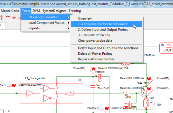
The results of the Efficiency Calculator are shown below. These results are calculated based on the average power dissipated by each component with a power probe attached to it.
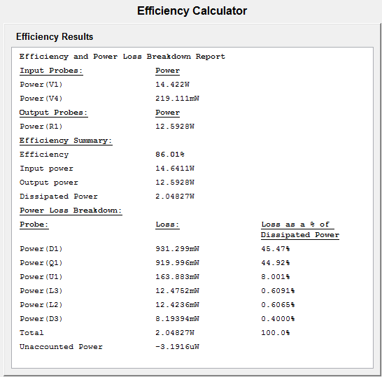
It cannot be emphasized strongly enough that for high efficiency conversion systems, getting accurate estimates of over all efficiency requires that the system be in steady state. Output transients must be fully settled out in order to obatin accurate results. Without a successful POP analysis, the user must exercise extreme patience in running long transients to allow the system reach steady state.
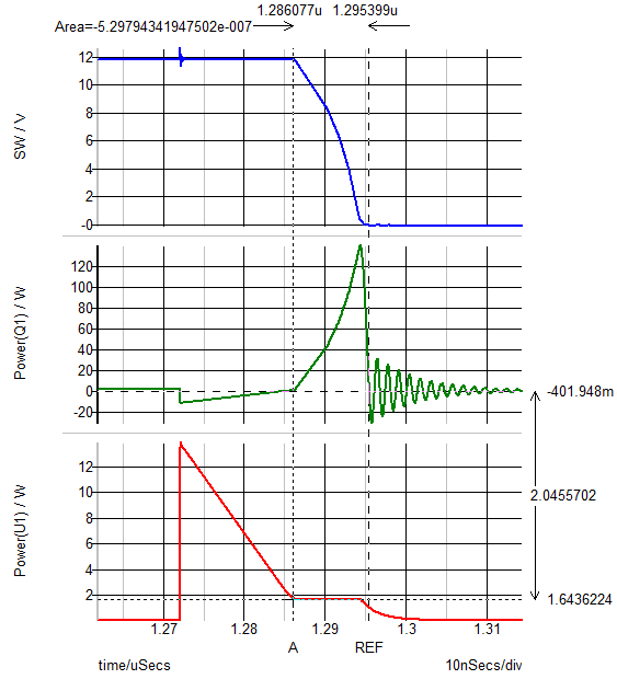
The above discussion focuses on average losses over a complete steady-state switching cycle. When optimizing the combined design of a driver and a MOSFET, we often need to look at the component portions of the switch losses, turn ON, turn OFF and conduction losses. There are a number of ways to do this. But one very easy one is shown here.
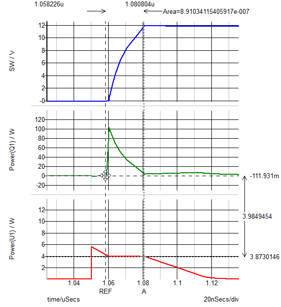
Note, that we have calculated the area under the instantaneous power dissipation curve for Q1 during the turn ON transition. To accomplish this, we set the cursors at the beginning and the end of the turn ON transition, and then double clicked on the time difference display. This action opens up a dialog window that allows us to request, the display of the area under the selected curve between the REF and A cursors.
The result is that we have now calculated the energy dissipated in the MOSFET during each turn ON transition. In this case, 0.89 uJ, which at 500 kHz results in a loss of 0.445 W.
Using the same approach to measure the turn OFF losses, we obtain 0.53uJ of turn OFF energy, which results in a loss of 0.265 W. The nice thing about this approach is that the designer can scale the loss results by the switching frequency, which can be very convenient when they are trying to optimize the overall design.
As is clear from the waveforms above, one would use the same approach to examine the losses in the driver circuit.
This modeling approach provides a powerful method for optimizing the design of a driver - power switch combination. The parameterization of the driver allows us to independently control the turn ON and turn OFF driver characteristics. The analysis approach allows us to optimize the driver characteristics, the power MOSFET selection according to the application requirements. This modeling approach for the driver is applicable to many different topologies and control laws.
Create a development testbench for your model at the very beginning.
Develop your model incrementally. Using the development testbench continuously test the model from the very beginning. Smaller quicker steps win the race.
It is OK to start out your model development with a flat schematic, but transition to a hierarchical schematic as early as feasible. Sooner is usually better. The half life of a large flat schematic is inversely proportional to ( the modeler's age - 30 )^2.
Create Testbenches for the final model and each critical component in it.
Measure the minimum time constant and number of New Topologies associated with the model
Measure the minimum time constant and number of New Topologies associated with the combination of the model and any other critical sources or loads. In this case, it is essential to characterize the driver model in combination with the level 2 MOSFET model.
|
© 2015 simplistechnologies.com | All Rights Reserved