SystemDesigner
SystemDesigner
|
The SystemDesigner D-to-A Converter (DAC) models a generic digital-to-analog converter. The input is a SystemDesigner bus, and the output is a ground-referenced analog voltage. The output can be gained and offset by the LSB weight and Output offset parameters.
The DAC continuously converts the input bus to an analog voltage. There is no sample and hold behavior; therefore, the DAC can be used whenever you need to convert a SystemDesigner Bus into an analog voltage. The SystemDesigner Bus Probe has the ability to convert a SystemDesigner bus to an analog voltage on a graph, eliminating the need for a DAC for probing purposes.
In this Topic Hide
Model Name: |
SystemDesigner D-to-A Converter |
|
Simulator: |
|
This device is compatible with the SIMPLIS simulator. |
Parts Selector |
SystemDesigner Functions (max. 32 bit) | A to D / D to A |
|
Symbol Library: |
SIMPLIS_SystemDesigner.sxslb |
|
Model File: |
SIMPLIS_SystemDesigner.lb |
|
Subcircuit Name: |
SIMPLIS_SD_DAC_32 |
|
Symbols: |
|
|
Multiple Selections: |
Only one device at a time can be edited. |
|
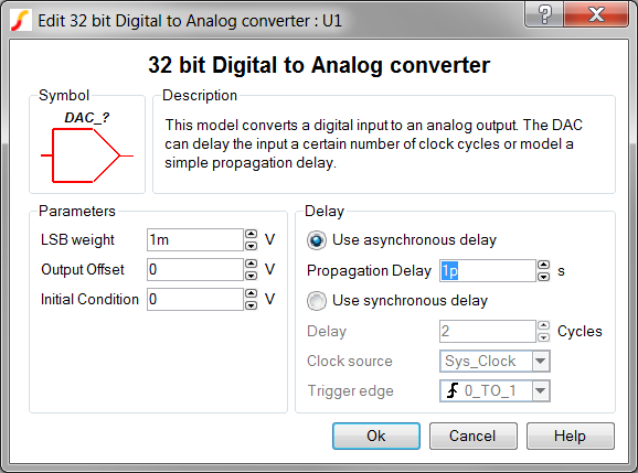
To configure the D-to-A Converter, double click the symbol to open the parameter editing dialog.
| Label | Parameter Description |
LSB weight |
The voltage amplitude which represents the least significant bit of the DAC |
Output Offset |
The input voltage which represents a zero output on the DAC. |
Initial Condition |
Initial condition of the output at time=0. Value is the output bus represented in decimal format. |
Use asynchronous delay |
Implements a combinatorial model where the output voltage changes in response to the input voltage(s) change after a propagation delay. |
Propagation Delay |
The propagation delay from an input change
to an output change in seconds. |
Use synchronous delay |
In response to an input voltage change, the output voltage changes after a designated number of clock cycles. |
Delay |
The propagation delay from an input change
to an output change in number of clock cycles. The output will
not change until the number of clock cycles has been reached.
The output will then change state only on the selected Clock
source edges specified by Trigger edge. |
Clock source |
|
Trigger edge |
|
The DAC circuit used to generate the following waveforms can be downloaded here: simplis_120_systemdesigner_dac_example.zip. In order to simulate this design, follow these steps:
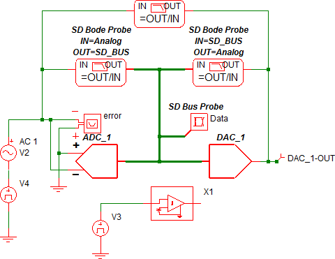
A similar example using the ADC can be downloaded here: simplis_119_systemdesigner_adc_example.zip
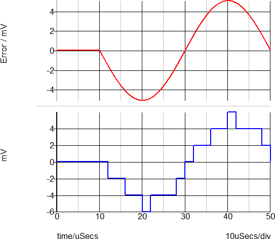
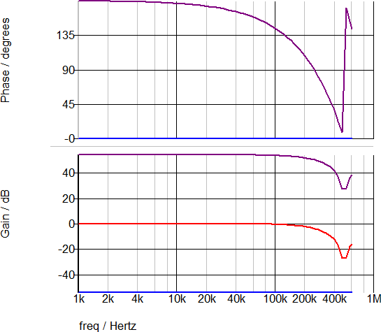
During integer-sampled data simulations, the sine wave voltage is sampled by the ADC and quantized into BIN_SIZE amplitude values. The BIN_SIZE is set to 2mV with a variable in the F11 window of the schematic. The quantized amplitude of the data signal has a maximum value of 3 LSB counts. The output signal is probed with the SystemDesigner probe labeled Data. The DAC then converts the Data value to an analog voltage. Because the gains of the ADC and the DAC are identical, the sampled voltage at the Data bus and the DAC output differ only by a propagation delay.
For double-precision floating-point sampled-data simulations, the DAC behaves as a pure gain. The AC Gain is simply the LSB Weight, and there is no phase change. The blue curves are the DAC Gain/Phase; the Purple curve is the ADC Gain/Phase; and the total Gain/Phase is represented by the red curves.
The AC transfer function for the adder is shown below. The DC gain is -54dB, ( BIN_SIZE ).
© 2015 simplistechnologies.com | All Rights Reserved

