SystemDesigner
|
This tutorial explains the following:
In this Topic Hide
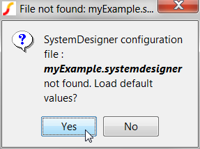
To start a new design, follow these steps.
Note: This tutorial uses myExample as the file name.
| Column | Value |
| Label | 2Meg |
| Frequency (Hz) | 2Meg |
Note: The default settings in the other columns are valid.
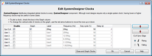
Note: You can return to the Edit SystemDesigner Clocks dialog to add or remove clocks; however, if you remove a clock, you must edit any SystemDesigner components that previously used that clock. In the future, an audit system will prevent you from simulating a design where a previously defined clock was used on a SystemDesigner component.
For more information about setting up clocks, see SystemDesigner Clocks.
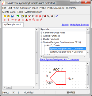
You can use the Parts Selector on the right side of the Schematic editor to place all SystemDesigner components. If the Parts Selector pane is hidden, click the blue Show Parts Selector link in the upper-right corner of the schematic.
All SystemDesigner
components are in the SystemDesigner
Functions (max. 32 bit)
section of the selection tree as shown below:
You have a choice of ways to select components to place on the schematic:
After you select a part, move your cursor onto the schematic and then click where you want to place that component.
To place parts for this tutorial example, follow these steps.
At this stage, the schematic should have three components and a ground symbol.
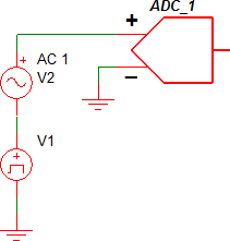
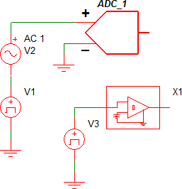
At this stage, you are ready to add two probes to view the output waveforms. Because SystemDesigner Buses, such as the output of the ADC, are treated differently than both analog voltages and other digital buses, special probes have been developed to probe the Bus signals.
To place the special probes, follow these steps using the Probes category in the SystemDesigner Functions (Max 32 bits) section of the Parts Selector.
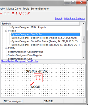
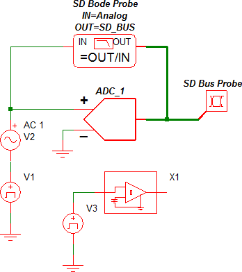
In the next section, you edit parameter values for four of the components and set up the analysis types.
If you are not sure about the purpose of a parameter as you edit the components, hover your mouse cursor over the parameter name or over the related text box or menu to view the associated tool tip.
To edit components for this tutorial example, follow these steps:
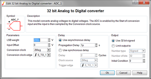
Note:The dialog box for each device that uses clocks is populated with values set in the SystemDesigner Clocks dialog. The default clock is the system clock (SysCLK) and is selected for this ADC. In the first procedure in this tutorial, you set the Label of the SysCLK to 2Meg which now appears in the Conversion Clock field and, in this tutorial, is appropriate for the design.
| Parameter | Value |
| Frequency | 1Meg |
| Pulse | 5 |
Note: When you change the Pulse value, the offset and Amplitude change automatically as shown below.
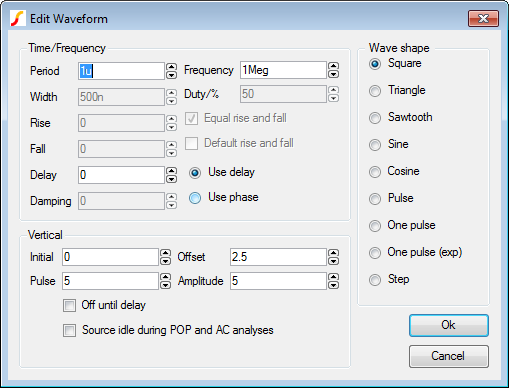
| Parameter | Value |
| Initial (voltage) | -1 |
| Wave shape | Sine |
| Source idle during POP and AC Analyses | Check |
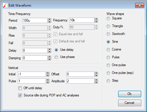
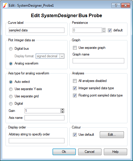
To set up the analysis types and set the analysis parameters, follow these steps:
| POP | AC | Transient |
| Select Use "POP Trigger" schematic device. | Stop Frequency = 10Meg | Stop time = 100u |
| Maximum Period = 1.1u |
A completed schematic example can be downloaded here: myExample.zip.
SIMPLIS SystemDesigner has two sampled-time
simulation modes: signed integer
and double-precision floating point.
The default sampled data type is Signed
Integer. The current default is labeled in the SystemDesigner
menu with => as shown below:

The following table lists the menu options to set a default simulation type from the SystemDesigner menu.
Mode |
To set default simulation |
| Signed integer | SystemDesigner | Set Default (F9) Sampled Data Type | Signed Integer |
Double-precision floating point |
SystemDesigner | Set Default (F9) Sampled Data Type | Double Precision Floating Point |
To run the default simulation, which, in this case, is the signed integer simulation, do one of the following:
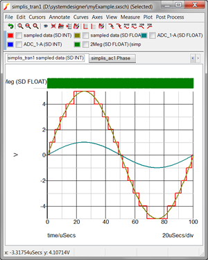
Signed-integer simulation results:
Running SystemDesigner with Signed Integer Data Type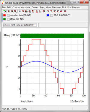
Note: In Step
2 of Editing_Component_Values,
you set the LSB weight of the ADC to 200mV. Since the input waveform
has a maximum amplitude of 1V, the maximum value of the time-sampled
output is +/-1V/200mV =+/- 5 LSBs.
Because the LSB weight of the ADC is large, not every sampling clock
creates a change in the ADC output; therefore, the sampling clock
has a higher frequency than the time-sampled output waveform.
To run the double-precision floating-point simulation, select SystemDesigner | Run w/ Sampled Data Type | Double Precision Floating Point from the menu bar.
Double-precision floating-point simulation results:
Running SystemDesigner with Double Precision Floating Point Data
	 Type
The
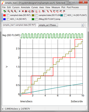
graph output has the results of the double-precision floating-point
simulation overlaid on the integer data results:
The olive curve shows the input voltage that is converted on every 2 MHz clock edge.
AC analysis results
To see the AC analysis results, click on the simplis_ac1 Phase tab:
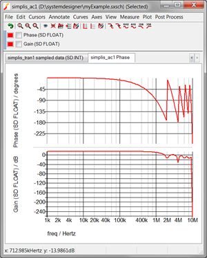
The SystemDesigner Bode Plot Probe is connected to probe the gain and phase of the transfer function of the ADC.
The theoretical transfer function is a gain with a zero-order sample and hold at the sampling clock frequency of 2MHz.
The low frequency gain should be 1/(LSB Weight) = 5 = 13.98dB.
The zero order sample and hold produces a phase wrap at the sampling frequency and at every harmonic higher than the sampling frequency as expected.
© 2015 simplistechnologies.com | All Rights Reserved