SIMPLIS Parts
SIMPLIS Parts
|
The Analog-to-Digital Converter (ADC) models a generic flash-type ADC.
Note: It is possible to start a new conversion before the previous conversion is complete if the next conversion starts more than the number of seconds specified by the Minimum Clock Width after the previous conversion started. The Minimum Clock Width must always be less than Convert Time. If the Minimum Clock Width specification is violated, the conversion does not start.
This model has a constant voltage reference. For an analog-to-digital converter with an adjustable voltage reference, see Analog-to-Digital Converter with Adjustable Voltage Reference.
In this Topic Hide
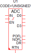
Model Name: |
Analog-to-Digital Converter |
|
Simulator: |
|
This device is compatible with the SIMPLIS simulator. |
Parts Selector |
Digital Functions | A to D / D to A |
|
Symbol Library: |
None - the symbol is automatically generated when placed or edited. |
|
Model File: |
None - the device model is generated before simulation. |
|
Subcircuit Name: |
SIMPLIS_DIGI1_D_A2D_CONVERTER_Y |
|
Symbols: |
|
|
Multiple Selections: |
Only one device at a time can be edited. |
|
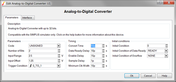
To configure the analog-to-digital converter, follow these steps:
| Label | Parameter Description | ||||||||||||
Code |
Encoding scheme for binary inputs of the ADC |
||||||||||||
Number of Bits |
Number of input bits for this A-to-D Converter |
||||||||||||
Input Range |
Analog input voltage range |
||||||||||||
Input Offset |
Midpoint of analog input voltage range |
||||||||||||
Trigger Condition |
Determines the triggering condition of the ADC clock pin:
|
||||||||||||
Convert Time |
Time required to convert analog input to digital output |
||||||||||||
Data Ready Delay |
Delay from when the output changes until the data-ready signal is true |
||||||||||||
Enable Delay |
Delay from when the enable pin goes active until the output is enabled |
||||||||||||
Sample Delay |
Time required to sample the analog input |
||||||||||||
Minimum Clock Width |
Minimum valid clock width |
||||||||||||
Initial Condition |
Initial condition of the converter output |
||||||||||||
Initial Condition of Data Ready |
Initial condition of the data ready output of a device |
||||||||||||
Initial Condition of Overflow |
Initial condition of the overflow outputs of the ADC
|
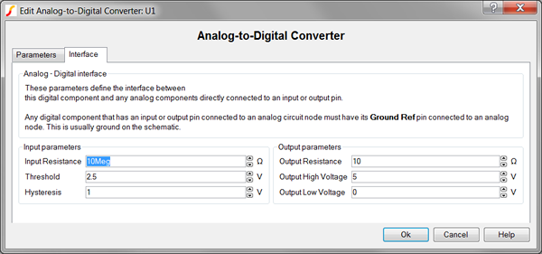
To define the parameters for the interface between this digital component and each analog component connected directly to an input or output pin, follow these steps from the Edit Analog-to-Digital Converter dialog box:
| Label | Parameter Description | |||||||
Input Resistance |
Input resistance of each input pin |
|||||||
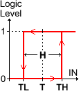
Threshold Hysteresis |
|
The Threshold (T) and Hysteresis (H) of the Schmitt trigger input buffer on each ADC input. To determine the low-to-high threshold (TH) and the high-to-low threshold (TL), substitute Threshold (T) and Hysteresis (H) in each of the following formulas :
|
||||||
Output Resistance |
||||||||
Output High Voltage |
||||||||
Output Low Voltage |
||||||||
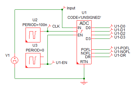
The test circuit used to generate the waveform examples in the next section can be downloaded here: simplis_060_adc_example.sxsch.
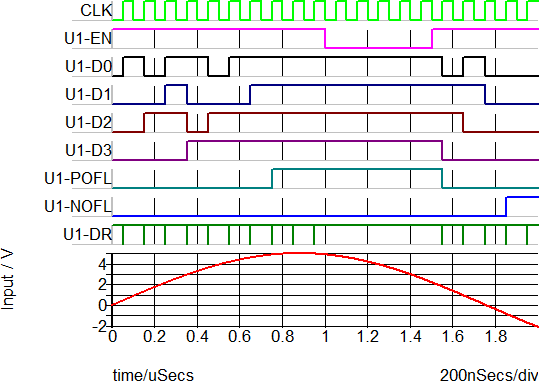
The waveforms below show the ADC operation with a sine-wave input.
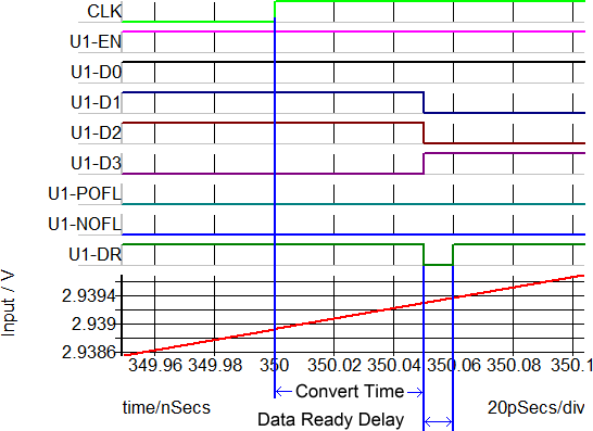
The timing waveforms pictured below show the detailed timing delays for the ADC.
Because this analog-to-digital converter model is generated by a template script when the simulation is executed, a fixed model cannot be inserted into a netlist. The template script for this device is simplis_make_a2d_model.sxscr, which you, as a licensed user, can download in a zip archive of all built-in scripts.
To download this zip file, follow these steps:
Note: You will be prompted to log in with the user name and password given to you when you registered.