SIMPLIS Parts
SIMPLIS Parts
|
The AND/NAND Gate models a generic AND or NAND gate with up to nine inputs. The number of active-low inputs can be set to one less than the total number of inputs. Both AND and NAND outputs are provided. The outputs change state at the same time, making the outputs perfectly complementary.
To implement a logic gate with more than nine inputs, see SIMPLIS Digital Lookup Table and SIMPLIS Lookup Table with Don't Care Input Definitions.
In this Topic Hide
Model Name: |
AND/NAND Gate |
|
Simulator: |
|
This device is compatible with the SIMPLIS simulator. |
Parts Selector |
Digital Functions | Gates |
|
Symbol Library: |
None - the symbol is automatically generated when placed or edited. |
|
Model File: |
SIMPLIS_DIGI1.lb |
|
Subcircuit Name: |
|
|
Symbol: |
|
|
Multiple Selections: |
Multiple AND gates can be selected and edited at the same time. |
|
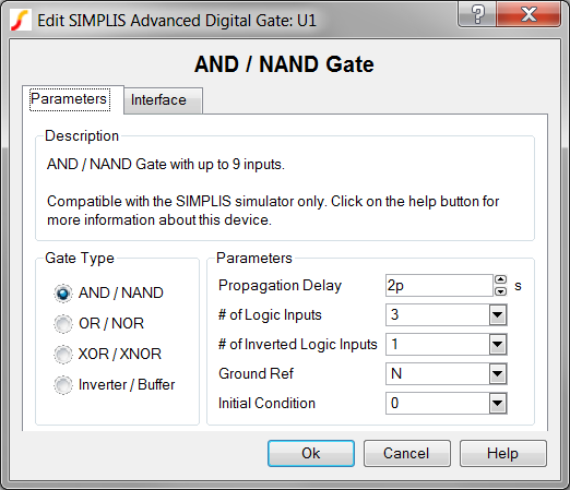
To configure the AND/NAND gate, follow these steps:
| Label | Parameter Description |
Propagation Delay |
Delay from when any input pin changes state until the outputs change state |
# of Logic Inputs |
Number of active-high logic inputs |
# of Inverted Logic Inputs |
Number of active-low logic inputs. Any device can have active-low inputs up to the # of Logic Inputs minus 1. |
Ground Ref |
Determines whether or not a device has a ground reference pin. |
Initial Condition |
Initial condition of the AND output at t=0 |
To define the parameters for the interface between this digital component and each analog component connected directly to an input or output pin, follow these steps from the Edit AND/NAND Gate dialog box:
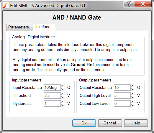
| Label | Parameter Description | |||||||
Input Resistance |
Input resistance of each input pin |
|||||||
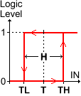
Threshold Hysteresis |
|
The Threshold (T) and Hysteresis (H) of the Schmitt trigger input buffer on each AND / NAND Gate input. To determine the low-to-high threshold (TH) and the high-to-low threshold (TL), substitute Threshold (T) and Hysteresis (H) in each of the following formulas :
|
||||||
Output Resistance |
||||||||
Output High Voltage |
||||||||
Output Low Voltage |
||||||||
The following truth table is for a two input AND/NAND gate with active-high inputs.
Inputs |
Outputs |
||
A |
B |
AND |
NAND |
0 |
0 |
0 |
1 |
0 |
1 |
0 |
1 |
1 |
0 |
0 |
1 |
1 |
1 |
1 |
0 |
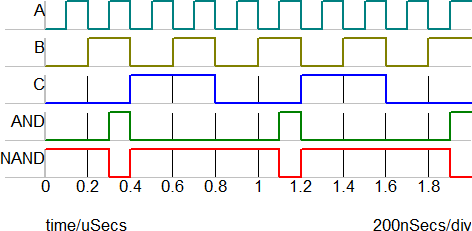
The test circuit used to generate the waveform examples in the next section can be downloaded here: simplis_056_andgate_example.sxsch.
The waveforms below were taken from a 3-input gate with two active-high inputs and one active-low input. The two active-high inputs are labeled A and B, and the active-low input is labeled C. With these connections, the AND output will be high when A and B inputs are high and the C input is low.
The subcircuit parameters, parameter names, data types, ranges, units, and descriptions are in the following table. The parameter names
can be used to directly generate netlist entries for the device. For example, the netlist entry for
a 3-input AND/NAND Gate with 1 inverted input and without ground reference would be as follows:
X$U1 6 9 2 3 4 SIMPLIS_DIGI1_AND3_N vars: NumInv=1 IC=0 RIN=10Meg ROUT=10 HYSTWD=1 VOL=0 VOH=5 DELAY=2p TH=2.5
| Parameter Name | Label | Data Type | Range | Units | Parameter Description | ||||||
NumInv |
# of Inverted Logic Inputs |
LIST |
0, |
Number of active-low logic inputs. Any device can have active-low inputs up to the # of Logic Inputs minus 1. |
|||||||
HYSTWD |
Hysteresis |
V |
The Threshold (T) and Hysteresis (H) of the Schmitt trigger input buffer on each AND / NAND Gate input. To determine the low-to-high threshold (TH) and the high-to-low threshold (TL), substitute Threshold (T) and Hysteresis (H) in each of the following formulas :
|
||||||||
IC |
Initial Condition |
LIST |
0, |
Initial condition of the AND output at t=0 |
|||||||
RIN |
Input Resistance |
min: 100 |
Ω |
Input resistance of each input pin |
|||||||
VOH |
Output High Voltage |
V |
|||||||||
VOL |
Output Low Voltage |
V |
|||||||||
ROUT |
Output Resistance |
min: 1m |
Ω |
||||||||
DELAY |
Propagation Delay |
1f to 1024 |
s |
Delay from when any input pin changes state until the outputs change state |
|||||||
TH |
Threshold |
V |
The Threshold (T) and Hysteresis (H) of the Schmitt trigger input buffer on each AND / NAND Gate input. To determine the low-to-high threshold (TH) and the high-to-low threshold (TL), substitute Threshold (T) and Hysteresis (H) in each of the following formulas :
|