SIMPLIS Parts
SIMPLIS Parts
|
The SIMPLIS MOSFET driver has multiple levels for use in different simulation objectives:
In this Topic Hide
Model Name: |
Multi-Level MOSFET Driver |
||
Simulator: |
|
This device is compatible with the SIMPLIS simulator. |
|
Parts Selector Menu Location: |
MOSFET Drivers ▶ Multi-Level MOSFET Driver |
||
Symbol Library: |
simplis_analog_functions.sxslb (some symbols are automatically drawn when placed) | ||
Model File: |
simplis_analog_functions.lb | ||
Subcircuit Name: |
SIMPLIS_MULTI_LEVEL_DRIVER | ||
Symbols: |
|
|
 |
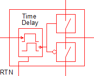
Level 0 |
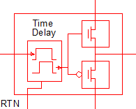
Level 1 |
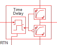
Level 2 |
|
Multiple Selections: |
Multiple devices can be selected and edited simultaneously. |
||
This symbol and the electrical model was introduced with version 8.0 and will not simulate in releases prior to Version 8.0.
For a MOSFET driver compatible with versions prior to version 8.0, see the parts selector entry:
Obsolete | MOSFET Drivers | Totem-Pole Output Driver (Obsolete)
The obsolete driver behaves like the Multi-Level MOSFET Driver when the level parameter is set to 0.
Symbols placed on schematics in previous versions of SIMetrix/SIMPLIS can be automatically migrated to use the new symbols. The schematic tools menu Tools ▶ Migrate Schematic Symbols to Version 8.00 will invoke a routine which migrates the existing symbols to the new symbols. As this action makes substantial changes to the schematic, it is recommended that you save a backup copy of the schematic first.
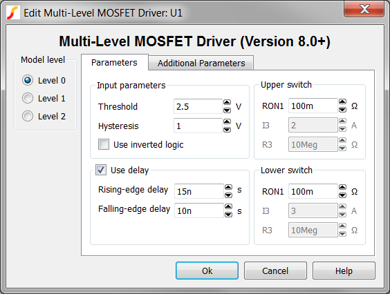
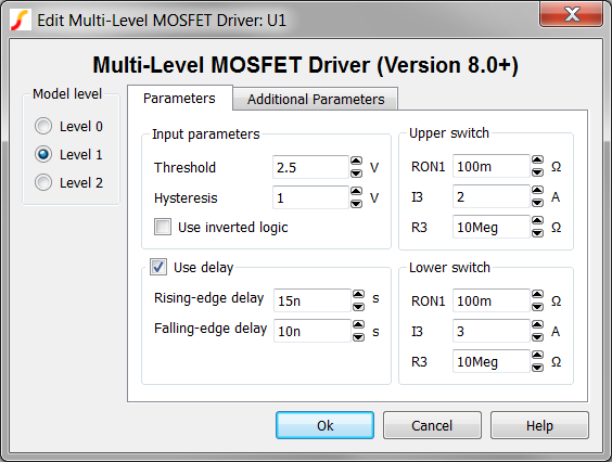
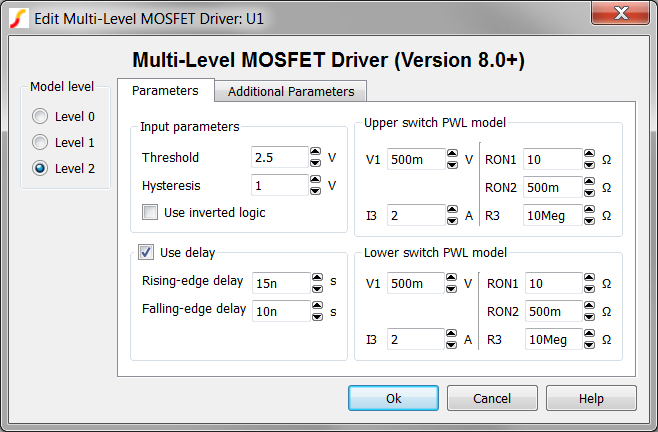
Parameters |
Units | Description |
| Input Parameters | ||
Threshold Hysteresis |
V |
The Threshold, in conjunction
with the Hysteresis parameter sets the input voltage thresholds: 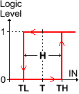
|
| Use Delay | n/a |
Determines whether or not to use a delay. |
| Rising-edge Delay | s |
The delay from the input rising edge to the initiation of output voltage change. The delay is independent of the logical inversion, and is always applied to the rising edge of the input. |
| Falling-edge Delay | s |
The delay from the input falling edge to the initiation of output voltage change. The delay is independent of the logical inversion and is always applied to the falling edge of the input. |
| Upper switch | ||
| RON1 | Ω |
The on resistance of the driver transistor. |
| Lower switch | ||
| RON1 | Ω |
The on resistance of the driver transistor. |
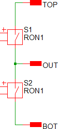
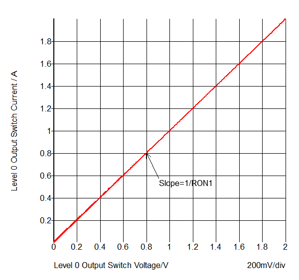
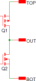
The Level 0 model uses simple switches with on resistance RON1. The output characteristics of one of these switches is shown below with a schematic diagram of the switch configuration.
 |
 |
Parameters |
Units | Description |
| Input Parameters | ||
Threshold Hysteresis |
V |
The Threshold, in conjunction
with the Hysteresis parameter sets the input voltage thresholds:
|
| Use Delay | n/a |
Determines whether or not to use a delay. |
| Rising-edge Delay | s |
The delay from the input rising edge to the initiation of output voltage change. The delay is independent of the logical inversion, and is always applied to the rising edge of the input. |
| Falling-edge Delay | s |
The delay from the input falling edge to the initiation of output voltage change. The delay is independent of the logical inversion and is always applied to the falling edge of the input. |
| Upper switch | ||
| RON1 | Ω |
The on resistance of the driver transistor. |
| I3 | A |
The peak current of the driver. |
| R3 | Ω |
The resistance of the driver transistor when the driver is sourcing the I3 current. This resistance is in parallel with the driver transistor. |
| Lower switch | ||
| RON1 | Ω |
The on resistance of the driver transistor. |
| I3 | A |
The peak current of the driver. |
| R3 | Ω |
The resistance of the driver transistor when the driver is sourcing the I3 current. This resistance is in parallel with the driver transistor. |
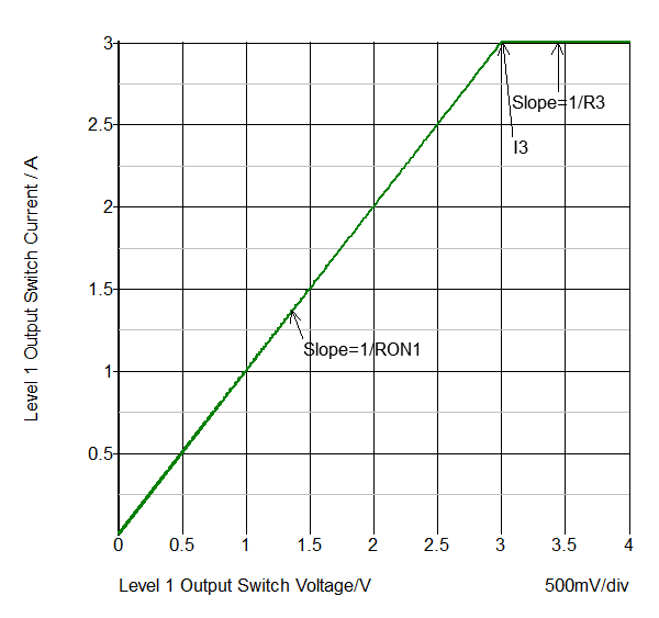
The Level 1 model uses transistor switches which model both on resistance RON1, and peak current I3. When the switch is sourcing/sinking the peak current, a parallel output resistance R3 is present across the switch terminals. The output characteristics of one of these switches is shown below with a schematic diagram of the switch configuration.
 |
 |
Parameters |
Units | Description |
| Input Parameters | ||
Threshold Hysteresis |
V |
The Threshold, in conjunction
with the Hysteresis parameter sets the input voltage thresholds:
|
| Use Delay | n/a |
Determines whether or not to use a delay. |
| Rising-edge Delay | s |
The delay from the input rising edge to the initiation of output voltage change. The delay is independent of the logical inversion, and is always applied to the rising edge of the input. |
| Falling-edge Delay | s |
The delay from the input falling edge to the initiation of output voltage change. The delay is independent of the logical inversion and is always applied to the falling edge of the input. |
| Upper switch PWL model | ||
| V1 | V |
The voltage where the driver transitions from the on resistance segment to the RON2 resistance segment. |
| I3 | A |
The peak current of the driver. |
| RON1 | Ω |
The on resistance of the driver transistor. |
| RON2 | Ω |
The resistance of the second segment in the PWL definition. |
| R3 | Ω |
The resistance of the driver transistor when the driver is sourcing the I3 current. |
| Lower switch PWL model | ||
| V1 | V |
The voltage where the driver transitions from the on resistance segment to the RON2 resistance segment. |
| I3 | A |
The peak current of the driver. |
| RON1 | Ω |
The on resistance of the driver transistor. |
| RON2 | Ω |
The resistance of the second segment in the PWL definition. |
| R3 | Ω |
The resistance of the driver transistor when the driver is sourcing the I3 current. |
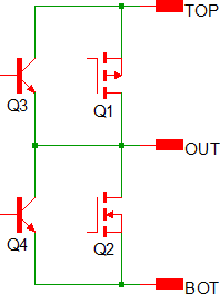
The Level 2 model uses PWL resistors to model the on resistance with two segments RON1 and RON2, and the peak current I3. When the switch is sourcing the peak current, a parallel output resistance R3 is present across the switch terminals. This model level can be used to model a composite NPN/MOSFET switch configuration as shown below with a schematic diagram below.
 |
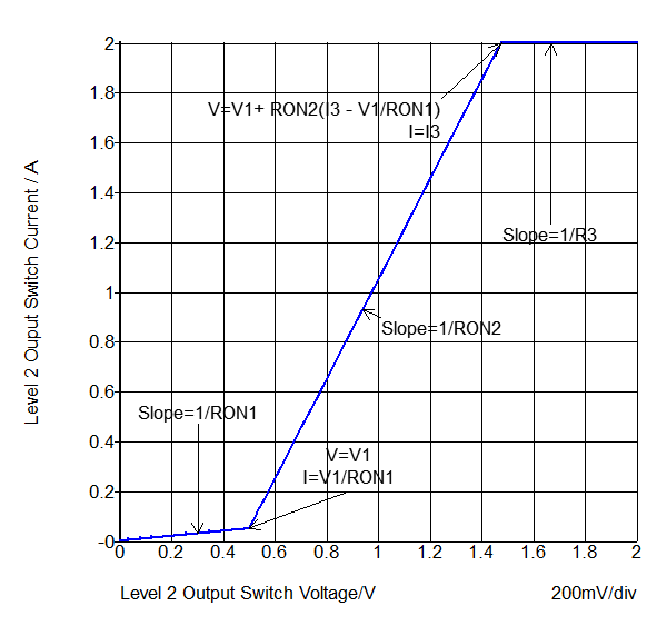 |
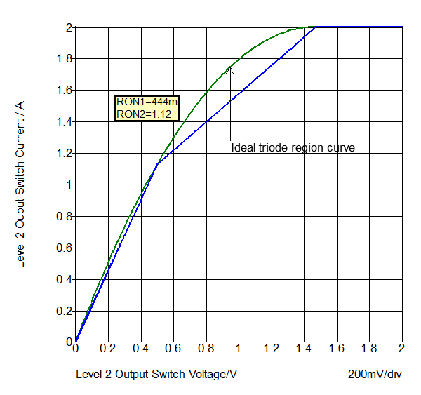
A more detailed MOSFET transistor can be modeled by changing the RON1 and RON2 parameters. In the below graph, the RON1 parameter is 444mΩ and the RON2 parameter to 1.12Ω.
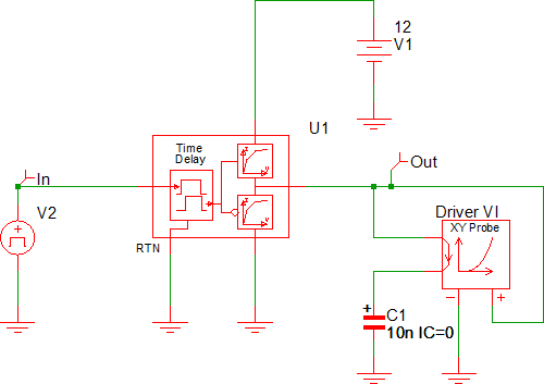
The test circuit used to generate the waveform examples in the next section can be downloaded here: simplis_068_multi_level_mosfet_driver.zip. Included in the zip archive is a schematic and the multi-step configuration file. The waveforms in the next section were taken from a multi-step simulation where the level parameter was stepped from 0 to 2, generating three output curves. Other than the level parameter, the driver uses the default values for all parameters. For information on the Multi-Step Analysis see Advanced SIMPLIS Training Course: 3.1 Multi-Step Simulations.
A similar driver is covered in the Advanced SIMPLIS Training Course: 7.0 MOSFET Driver Model.
The MOSFET driver output waveforms for each of the three model levels is shown below.
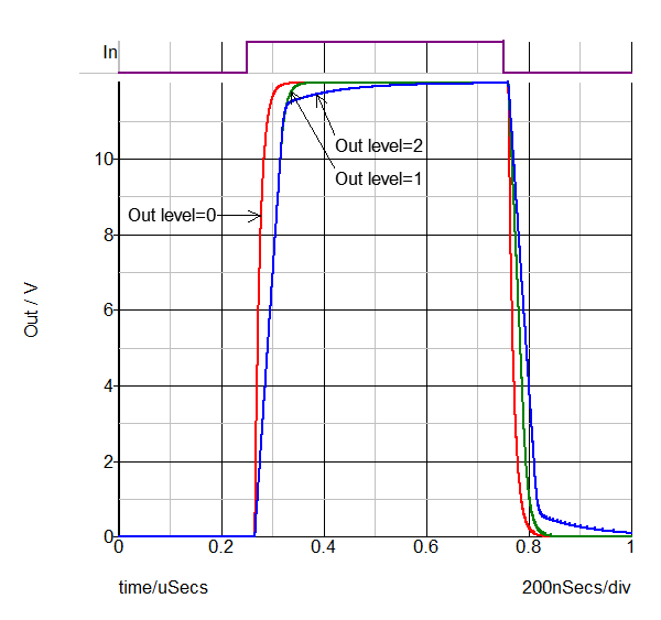
The MOSFET Driver output current is plotted against the output voltage in the graph below. This graph is useful to gain an in-depth understanding how the driver works.
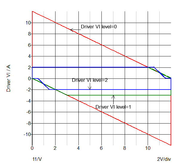
Following the red curve which is for the Level 0 model, the driver starts with the output voltage at 0V and driver current at 0A.
The green curve is for the Level 1 model.
The blue curve is for the Level 2 model.
© 2015 simplistechnologies.com | All Rights Reserved