DVM - Design Verification Module
DVM - Design Verification Module
|
The purpose of the BodePlot() test is to measure the control-loop stability. The input is configured as a DC Input Source, and the output is configured as a special BodePlot Load with a small-signal AC source and a Bode Plot probe. Since the test objective does not specify the input voltage nor the output current, you must provide these values in the Source and Load columns in the testplan.
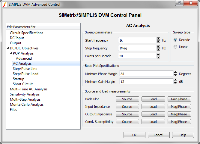
Both a POP and an AC analysis are used in the BodePlot() test.
The POP and AC analysis directives are taken from the POP Analysis page and the AC Analysis page of the Full Power Assist DVM control symbol. The AC Analysis page is shown below.
The test report includes gain, phase, source, and load graphs as well as the following scalar values which are defined in the Measured Scalar Values section below:
|
|
In this Topic Hide
The BodePlot() function has the following syntax with the argument described in the table below:
BodePlot(REF)
| Argument | Range | Description |
| REF | n/a | The actual reference designator of the DVM Load or the generic syntax of OUTPUT:n where n is an integer indicating a position in the list of managed DVM loads. |
The BodePlot() test objective sets the source and load subcircuits to the following:
| Source | Load |
| DC Input Source | Bode Plot Load |
Loads other than the output under test are set to the Resistive Load. All other sources are set to the DC Input Source.
The BodePlot() test objective measures the following scalar values,where {load_name} and {src_name} are replaced by the actual load name source name:
| Scalar Name | Description | ||||||||||||
| Efficiency | The overall efficiency of the converter taken from the POP simulation | ||||||||||||
| Power({load_name) | The power of each input source taken from the POP simulation | ||||||||||||
| Power({load_name}) | The power of each output load taken from the POP simulation | ||||||||||||
| gain_crossover_freq | The frequency where the gain of the control loop is 0 dB | ||||||||||||
| gain_margin | The gain margin when the phase change in the control loop is 180 degrees. | ||||||||||||
| min_phase | The minimum value for the phase during the AC analysis | ||||||||||||
| phase_crossover_freq | The frequency where the phase change in the control loop is 180 degrees. | ||||||||||||
| min_phase_freq | The frequency where the phase is at its minimum value | ||||||||||||
| phase_margin | The phase when the gain of the control loop is 0 dB | ||||||||||||
| sw_freq | A number which represents the converter switching frequency. This scalar is generated from a fixed probe with curve label DVM Frequency. For more information, see Measuring the Switching Frequency. | ||||||||||||
|
The Average, Minimum, Maximum, RMS and Peak-to-Peak values for each load voltage and current taken over the entire simulation time window. | ||||||||||||
|
The Average, Minimum, Maximum, RMS and Peak-to-Peak values for each source voltage and current taken over the entire simulation time window. |
In the following table, {load_name} is the name assigned to each load. The default value is LOAD. DVM forces each load name to be unique so that the scalar and specification values for each load are unique.
| Specification Name | PASS/FAIL Criteria |
| Min_V{load_name} | The minimum value of the output voltage during the simulation time is greater that the minimum specification value. |
| Max_V{load_name} | The maximum value of the output during the simulation time is less than the maximum specification value. |
| min_gain_margin | The minimum value of the gain margin during the AC analysis is greater than minimum specification value. |
| min_phase_margin | The minimum value of the phase margin during the AC analysis is greater than minimum specification value. |
The BodePlot() test objective is used in several built-in testplans. Shown below is a test from the DC/DC 1 input/1 output testplan. The source and load are defined in the Full Power Assist DVM control symbol. The test configures the source to use the Nominal symbolic value from the DC Input page and configures the load based on the Light symbolic value from the Output page.
| *?@ Analysis | Objective | Source | Load | Label |
| Ac | BodePlot(OUTPUT:1) | SOURCE(INPUT:1, Nominal) | LOAD(OUTPUT:1, Light) | Ac Analysis|Bode Plot|Vin Nominal|Light Load |
You can view the complete test report in a new browser window here: BodePlot Test Report. Below is an interactive link to the same test report.
© 2015 simplistechnologies.com | All Rights Reserved