SIMPLIS Parts
SIMPLIS Parts
|
Any SPICE MOSFET model installed in the SIMetrix library can be converted for use in SIMPLIS. When a MOSFET is placed on a SIMPLIS schematic, a model parameter extraction routine is invoked to automatically convert the SPICE model to a SIMPLIS model. During the model parameter extraction process, SIMetrix/SIMPLIS automatically runs several SPICE simulations on the SPICE model and extracts the SIMPLIS model parameters. After the Piecewise Linear (PWL) model parameters have been extracted, the resulting MOSFET model will run in SIMPLIS.
In this Topic Hide
When you place a MOSFET symbol on a schematic, the Extract MOSFET Parameters dialog opens for you to edit the default test conditions. You should change the test conditions to accurately reflect the expected voltage, current, and temperature of the device in your circuit.
The default test conditions are defined using the command shell menu, File ▶ Options ▶ SIMPLIS Options.... For additional information, see SIMPLIS MOSFET Options.
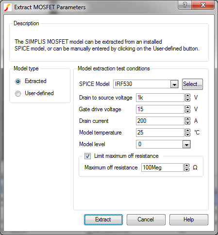
The following table describes the Extract MOSFET Parameters dialog test
conditions.
| Test Condition | Default Value | Units | Description |
|---|---|---|---|
| SPICE Model | IRF530 | The SPICE model used to extract SIMPLIS parameters. |
|
| Model type | Extracted | Invokes the model parameter extraction algorithms. |
| Drain to source voltage | 1k |
V |
The peak off-state voltage seen by this device. Used to extract capacitance for model levels which include parasitic capacitance. Breakdown is not modeled. |
| Gate drive voltage | 15 |
V |
Gate to source voltage to extract RDS(on). |
| Drain Current | 200 |
A |
Peak drain current to extract the RDS(on) and forward gain of the MOSFET. |
| Model temperature | 25 |
°C |
Temperature used for all extraction simulations. |
| Model level | 0 |
Model complexity. For information on choosing the model level, see MOSFET Model Levels. |
|
| Limit maximum off resistance | Checked |
none |
Limits the off resistance for the MOSFET. For some SPICE models, this will produce a SIMPLIS model which runs faster. |
| Maximum off resistance | 100Meg |
W |
The maximum off resistance of the MOSFET switch. This value is used only if "Limit maximum off resistance" is checked. |
The SIMPLIS MOSFET models have multiple levels to balance simulation speed vs. model accuracy. There are currently four levels: 0, 1, 2, and 3. As the model level increases, so does the model complexity and, as a rule, simulation times also increase.
SIMPLIS extracts a model based on the model level chosen in the Extract MOSFET Parameters dialog. Currently model levels 0, 1, and 2 are supported by the model parameter extraction algorithms. The level 3 model is intended for more detailed modeling and can be manually generated from a device datasheet or from a spreadsheet or other program. For details of the Level 3 model, see Manually Generate and Customize MOSFET Models. Although these models are internally saved as ASCII text, the following illustrations show the three model levels in a schematic form.
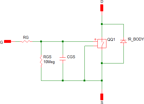
Level 0 models a switch with on/off resistance values, a body diode, gate resistance, and gate-to-source capacitance. The Level 0 Model can be used for AC Bode Plots and for simulating output voltage during load and line transients when the actual switching waveform shapes are not critical.
Below is a schematic view of a Level 0 model:
| Level 0 models these circuit elements | Level 0 Schematic | ||||||||||
|
 |
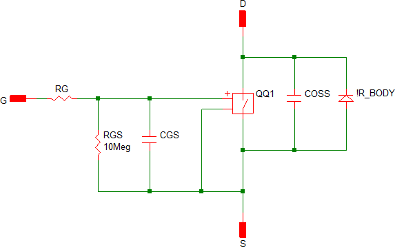
Level 1 models a switch with on/off resistance values, a body diode, gate resistance, gate-to-source capacitance, plus a lumped-linear Coss capacitance across drain and source terminals. The Level 1 Model can be used for power stage simulations, including Quasi-resonant, LLC, and phase-shifted bridge topologies,as well as for AC Bode Plots and for simulating output voltage during load and line transient.
Below is a schematic view of a Level 1 model:
| Level 1 models these circuit elements | Level 1 Schematic | ||||||||||||
|
 |
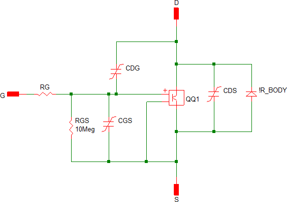
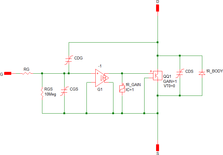
Level 2 models a switch with forward transconductance gain, a body diode, and gate-to-source capacitance, plus a nonlinear Gate-Drain, Drain-Source, and Gate-Source capacitors. The active region is modeled by a linear transconductance gain (ID is proportional to VGS - VT0). The Level 2 Model can be used for switching losses, MOSFET voltage and current stresses, and all simulations covered by Level 0 and Level 1 models.
Below is a schematic view of Level 2 model:
| Level 2 models these circuit elements | Level 2 Schematic | ||||||||||||||
|
 |
The Level 3 model extends the Level 2 model to include up to 5 forward transconductance gain segments. The Level 3 model can be used to more accurately model converter losses for converters which operate over a wide range of currents.
Note: The model extraction algorithms do not extract a level 3 model. The level 3 model is available for manually generated models. See Manually Generate and Customize MOSFET Models for details.
Below is a schematic view of a Level 3 Model:
| Level 3 models these circuit elements | Level 3 Schematic | ||||||||||||||||||
|
 |
The user-defined model uses parameters entered directly in the Edit MOSFET Parameters dialog without invoking the model extraction algorithms. A MOSFET can be switched from an extracted model to a user-defined model at any point; however the extracted parameters are by default copied over to the user-defined parameters, replacing any user-entered values. You can disable this behavior in the SIMPLIS Options dialog by clearing the check box labeled "Automatically copy extracted parameters to User-defined parameters." You can access these options from the command shell menu File ▶ Options ▶ SIMPLIS Options.... For more information, see SIMPLIS MOSFET Options.
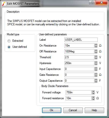
The following table describes the Edit MOSFET Parameters entries for a User-defined model.
| Parameters | Default Value | Units | Description |
|---|---|---|---|
| Label: | USER_LABEL | Any descriptive text. Cannot contain whitespace characters. | |
| Model type | User-defined | The values in this dialog are used literally. | |
| On Resistance: | 10m | W | The on resistance of the MOSFET switch. |
| Off Resistance: | 100Meg | W | The off resistance of the MOSFET switch |
| Threshold: | 2.5 | V | MOSFET
threshold voltage - the MOSFET will turn on at (Threshold
+ 1/2 Hysteresis). Turn off occurs at (Threshold - 1/2 Hysteresis). |
| Hysteresis: | 250m | V | The hysteresis of the MOSFET |
| Input Capacitance: | 0 | F | The input capacitance ( CGS) of the MOSFET. Set to 0 to remove the capacitor from the model. |
| Gate Resistance: | 0 | W | The internal resistance of the MOSFET. Set to 0 to remove the gate resistance from the model. |
| Output Capacitance: | 0 | F | A
non-zero value will place a linear capacitance between the MOSFET
drain and source terminals. Set to 0 to remove capacitor from the model. |
| Body Diode Parameters | |||
| Forward voltage: | 750m | V | Diode forward voltage drop. The diode effectively turns on at this voltage. |
| Forward resistance: | 10m | W | The Body Diode resistance at voltages higher than the Forward voltage |
| Models these circuit elements | User-defined Schematic | ||||||||||||
|
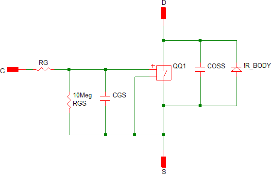 |
You can customize or manually generate your own MOSFET models using a parameter string with multiple PARAM_NAME=PARAM_VALUE key-value pairs. The parameter names and their functions are described in the MOSFET Model Parameters section below. You can interpret the SIMPLIS parameter values from device datasheet specifications and curves.
You can compose the parameter string in a text editor, spreadsheet, or script. The order of the parameter names in the parameter string and the capitalization of the parameter names are irrelevant.
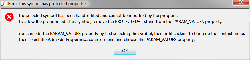
You can include a PROTECTED=1 key-value pair to prevent from extracting a model and overwriting your manually generated parameters. The PROTECTED=1 key-value pair is not used in the simulation.
Note: When you
click on the device after adding the PROTECTED=1 key-value pair, the following
message box appears to warn you that this is a hand-edited model.
To customize or generate your own MOSFET model, follow these steps:
Alternately you can write the PARAM_VALUES property to the symbol using
the Prop command in the command line with the following syntax:
prop PARAM_VALUES parameter_string
where parameter_string is the set of
key-value pairs that you created in Steps 1
and 2 above. Since parameter_string contains spaces, the entire
string must be enclosed in double quotes.
The following tables detail the parameters which define the electrical behavior of the MOSFET model. Several other parameters in the PARAM_VALUES property have no effect on the electrical behavior of the model. These parameters are used to populate the Extract MOSFET Parameters dialog box.
Note: The default values are unlikely to appear in an extracted model. If these parameter values appear in your design, there has been an error in composing the parameter string.
| Parameter Name | Default Value | Description |
| LEVEL | 0 | Model Level |
| RDSON | 10m | Switch QQ1 On resistance |
| ROFF | 100Meg | Switch QQ1 Off Resistance |
| VT0 | 2.5 | Switch QQ1 Threshold |
| HYSTWD | 1 | Switch QQ1 Hysteresis |
| RG | 1.123456789 | Gate Resistance |
| Parameter Names | Default Value | Description | |
| GAIN_NSEG | 2 (off and on) | Number of segments in the Gain model | |
| VT0 | 1.123456789 | X-Y point definitions for gain:
The parameters listed in green are used only in Level=3 models. |
|
| VGS2 | ID2 | 1.123456789 | |
| VGS3 | ID3 | 1.123456789 | |
| VGS4 | ID4 | 1.123456789 | |
| VGS5 | ID5 | 1.123456789 | |
| Parameter Names | Default Value | Description | |
| BD_NSEG | 3 | Number of segments in the body diode model.
|
|
| VD0 | IBD0 | 1.123456789 | X-Y point definitions for body diode:
|
| VD1 | IBD1 | 1.123456789 | |
| VD2 | IBD2 | 1.123456789 | |
| VD3 | IBD3 | 1.123456789 | |
| VD4 | IBD4 | 1.123456789 | |
| VD5 | IBD5 | 1.123456789 | |
| VD6 | IBD6 | 1.123456789 | |
Capacitors are modeled in SIMPLIS with Piece-Wise Linear capacitors.
| Parameter Names | Default Value | Description | |
| CGS_NSEG | 1 | Number of segments in the Gate-Source capacitor model | |
| VCGS0 | QCGS0 | 1.123456789 | X-Y point definitions for CGS:
|
| VCGS1 | QCGS1 | 1.123456789 | |
| VCGS2 | QCGS2 | 1.123456789 | |
| VCGS3 | QCGS3 | 1.123456789 | |
| VCGS4 | QCGS4 | 1.123456789 | |
| VCGS5 | QCGS5 | 1.123456789 | |
| VCGS6 | QCGS6 | 1.123456789 | |
| VCGS7 | QCGS7 | 1.123456789 | |
| VCGS8 | QCGS8 | 1.123456789 | |
| VCGS9 | QCGS9 | 1.123456789 | |
| VCGS10 | QCGS10 | 1.123456789 | |
| Parameter Names | Default Value | Description | |
| CDS_NSEG | 4 | Number of segments in the Drain-Source capacitor model | |
| VCDS0 | QCDS0 | 1.123456789 | X-Y point definitions for CDS:
|
| VCDS1 | QCDS1 | 1.123456789 | |
| VCDS2 | QCDS2 | 1.123456789 | |
| VCDS3 | QCDS3 | 1.123456789 | |
| VCDS4 | QCDS4 | 1.123456789 | |
| VCDS5 | QCDS5 | 1.123456789 | |
| VCDS6 | QCDS6 | 1.123456789 | |
| VCDS7 | QCDS7 | 1.123456789 | |
| VCDS8 | QCDS8 | 1.123456789 | |
| VCDS9 | QCDS9 | 1.123456789 | |
| VCDS10 | QCDS10 | 1.123456789 | |
| Parameter Names | Default Value | Description | |
| CDG_NSEG | 4 | Number of segments in the Drain-Gate capacitor model | |
| VCDG0 | QCDG0 | 1.123456789 | X-Y point definitions for Drain-Gate capacitor:
|
| VCDG1 | QCDG1 | 1.123456789 | |
| VCDG2 | QCDG2 | 1.123456789 | |
| VCDG3 | QCDG3 | 1.123456789 | |
| VCDG4 | QCDG4 | 1.123456789 | |
| VCDG5 | QCDG5 | 1.123456789 | |
| VCDG6 | QCDG6 | 1.123456789 | |
| VCDG7 | QCDG7 | 1.123456789 | |
| VCDG8 | QCDG8 | 1.123456789 | |
| VCDG9 | QCDG9 | 1.123456789 | |
| VCDG10 | QCDG10 | 1.123456789 | |
© 2015 simplistechnologies.com | All Rights Reserved