SIMPLIS Parts
SIMPLIS Parts
|
The default test conditions for the Extract MOSFET Parameters dialog can be set from the Command Shell menu File ▶ General ▶ SIMPLIS Options..... Three advanced options are hidden by default until you click the Show Advanced Options button.
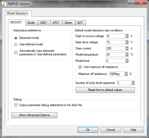
| Test Condition | Default Value | Units | Description |
|---|
| Drain to source voltage | 1k |
V |
The peak off-state voltage seen by this device. Used to extract capacitance for model levels which include parasitic capacitance. Breakdown is not modeled. |
| Gate drive voltage | 15 |
V |
Gate to source voltage to extract RDS(on). |
| Drain Current | 200 |
A |
Peak drain current to extract the RDS(on) and forward gain of the MOSFET. |
| Model temperature | 25 |
°C |
Temperature used for all extraction simulations. |
| Model level | 0 |
Model complexity. For information on choosing the model level, see MOSFET Model Levels. |
|
| Limit maximum off resistance | Checked |
none |
Limits the off resistance for the MOSFET. For some SPICE models, this will produce a SIMPLIS model which runs faster. |
| Maximum off resistance | 100Meg |
W |
The maximum off resistance of the MOSFET switch. This value is used only if "Limit maximum off resistance" is checked. |
| Option | Default Value | Description |
|---|---|---|
Initial Place Preference |
Extracted |
Indicates which model type (Extracted or User-defined) is selected when you place the device on the schematic. |
Automatically copy extracted parameters to User-defined parameters |
Checked |
If checked the extracted parameters overwrite the user-defined parameters each time a model is extracted. If unchecked, the user-defined parameters are never overwritten. |
Number of body diode segments |
3 |
Sets the number of segments for the Body diode extraction algorithm. If you select 2, the algorithm models on and off resistance. If you select 3, the algorithm models a transition resistance in between the on and off segments. |
Debug |
||
Output parameter ... |
Unchecked |
If checked, the debug statements are automatically written to the deck file. The Command shell menu SIMPLIS ▶ Edit Netlist (after preprocess) opens the .deck file for editing. An example set of debug statements can be found in the Deck-Level Debug section. |
Advanced options |
Hidden |
Click this button to view or change the advanced options. For more information, see Advanced Options. |
If you check "Output parameter debug statements to the deck file," each MOSFET in the design has a debug report inserted in the .deck file when you run a simulation. This debug report displays the calculated values for each major parameter in a formatted table. You can edit the .deck file with the Command shell menu SIMPLIS ▶ Edit Netlist (after preprocess). A sample debug report is shown below:
***SIMPLIS
DEBUG EXTRACTED MOS START********************************************
*** ***
*** Device with REF : Q1 ***
*** ***
*** Extracted from SPICE model: IRF530 ***
*** ***
********************************************************************************
*
* Model Extraction Parameters
*
* VD_PEAK : 900
* ID_PEAK : 28
* VGSON :
15
* TEMP :
25
* LEVEL :
0
* POL :
1
* LIMIT_MAX_ROFF : 1
* MAX_ROFF : 100Meg
*
*
* Conduction Parameters
*
* RDSON : 125.171m
* ROFF : 100Meg
*
* Forward Gain Parameters
*
* VT0 : 4.98562
* HYSTWD : 498.562m
*
* Body Diode Parameters
*
* BD_NSEG : 4
* R BODY SEG#1 : 1
* R BODY SEG#2 : infinite
* R BODY SEG#3 : 35.7196m
* R BODY SEG#4 : 15.9721m
*
* Body Diode V-I Conduction Points
*
* VD0 : -10.001k
* IBD0 : -1
* VD1 : -10k
* IBD1 : 0
* VD2 : 680.304m
* IBD2 : 0
* VD3 : 816.14m
* IBD3 : 3.80284
* VD4 : 1.20262
* IBD4 : 28
*
* Gate Resistance
*
* RG : 973.603m
*
* Gate - Source Capacitance Parameters
*
* CGS : 616.999p
*
* Drain - Gate Capacitance Parameters
*
* CDG SEG#1 : 173.8p
* CDG SEG#2 : 41.7796p
* CDG SEG#3 : 33.7874p
* CDG SEG#4 : 31.6724p
*
* Drain - Gate Charge V-Q Points
*
* CDG_NSEG : 4
* VCDG0 : 0
* QCDG0 : 0
* VCDG1 : 19.2895
* QCDG1 : 3.35252n
* VCDG2 : 214.212
* QCDG2 : 11.4963n
* VCDG3 : 360
* QCDG3 : 16.4221n
* VCDG4 : 900
* QCDG4 : 33.5252n
*
*
* Drain - Source Capacitance Parameters
*
* CDS SEG#1 : 99.1877p
* CDS SEG#2 : 31.3306p
* CDS SEG#3 : 14.3872p
* CDS SEG#4 : 9.5245p
*
* Drain - Source Charge V-Q Points
*
* CDS_NSEG : 4
* VCDS0 : 0
* QCDS0 : 0
* VCDS1 : 13.7018
* QCDS1 : 1.35905n
* VCDS2 : 137.995
* QCDS2 : 5.25323n
* VCDS3 : 360
* QCDS3 : 8.44727n
* VCDS4 : 900
* QCDS4 : 13.5905n
*
********************************************************************************
*** ***
*** Device with REF : Q1 ***
*** ***
*** Extracted from SPICE model: IRF530 ***
*** ***
***SIMPLIS DEBUG EXTRACTED MOS END**********************************************
© 2015 simplistechnologies.com | All Rights Reserved