SIMPLIS Parts
SIMPLIS Parts
|
The Shift Register models a combination of a clocked data type register and a shift register. The clock edge for the register can be set with the Trigger Condition parameter to be a rising edge (0_TO_1) or a falling edge (1_TO_0). The set and reset inputs can be either asynchronous or synchronous, depending on the Set/Reset Type parameter. The active logic level of the inputs can be configured with the Set/Reset Level and Load/Shift Level parameters.
For the shift register with both asynchronous and synchronous set and reset inputs, see Shift Register with both Async and Sync Set/Reset.
Related topics:
In this Topic Hide
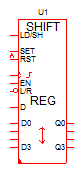
Model Name: |
Shift Register |
|
Simulator: |
|
This device is compatible with the SIMPLIS simulator. |
Parts Selector |
Digital Functions | Registers |
|
Symbol Library: |
None - the symbol is automatically generated when placed or edited. |
|
Model File: |
None - the device model is generated before simulation. |
|
Subcircuit Name: |
|
|
Symbol: |
|
|
Multiple Selections: |
Only one device at a time can be edited. |
|
To configure the shift register, follow these steps:
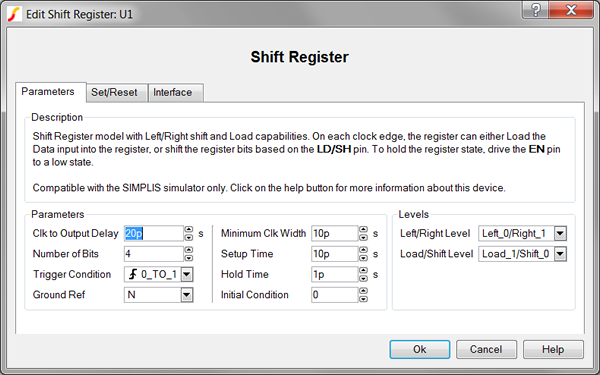
| Label | Parameter Description |
Clock to Output Delay |
|
Number of Bits |
Number of input and output bits for the shift register |
Trigger Condition |
Determines the triggering condition of the shift register clock pin:
|
Ground Ref |
Determines whether or not a device has a ground reference pin. |
Minimum Clock Width |
Minimum valid clock width. Clock widths less than this parameter will not trigger the shift register. |
Setup Time |
|
Hold Time |
|
Initial Condition |
Initial condition of the shift register output in decimal |
Left/Right Level |
Determines the logic level of the shift register left/right (L/R) pin:
|
Load/Shift Level |
Determines the logic level of the shift register load/shift (LD/SH) pin:
|
To define the set/reset behavior of the shift register, follow these steps from the Shift Register dialog box:
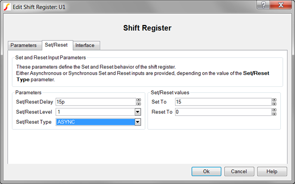
| Label | Parameter Description | ||||||
Set/Reset Delay |
Delay from when the set or reset pin goes active until the output is actually set or reset. The Set/Reset Delay is used only for asynchronous set/reset. Registers with synchronous set/reset use the Clock to Output Delay. |
||||||
Set/Reset Level |
|
||||||
Set/Reset Type |
|
||||||
Set To |
Determines the shift register output value when the set pin goes active |
||||||
Reset To |
Determines the shift register output value when the reset pin goes active |
To define the parameters for the interface between this digital component and each analog component connected directly to an input or output pin, follow these steps from the Shift Register dialog box:
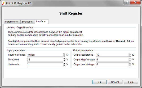
| Label | Parameter Description | |||||||
Input Resistance |
Input resistance of each input pin |
|||||||
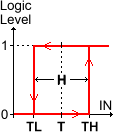
Threshold Hysteresis |
|
The Threshold (T) and Hysteresis (H) of the Schmitt trigger input buffer on each Register input. To determine the low-to-high threshold (TH) and the high-to-low threshold (TL), substitute Threshold (T) and Hysteresis (H) in each of the following formulas :
|
||||||
Output Resistance |
||||||||
Output High Voltage |
||||||||
Output Low Voltage |
||||||||
The two truth tables below show the logic behavior with asynchronous and synchronous set/reset.
The following truth table assumes these parameter values:
When the EN input is high, and the Load/Shift Level=Load_1/Shift_0, the Register will Load the D input when the LD/SH pin is high, and Shift the Q output when the LD/SH pin is low.
Inputs |
Output |
Action |
||||||
LD/SH |
ASET |
ARST |
EN |
L/R |
D |
CLK |
Q |
|
0 |
0 |
0 |
 |
Last Q |
Retain state |
|||
1 |
0 |
0 |
1 |
|
Data input |
Load data |
||
0 |
0 |
0 |
1 |
0 |
0 |
|
Q = Last Q shifted left, LSB=0 |
Shift left |
0 |
0 |
0 |
1 |
1 |
0 |
|
Q = Last Q shifted right, MSB=0 |
Shift Right |
0 |
0 |
0 |
1 |
0 |
1 |
|
Q = Last Q shifted left, LSB=1 |
Shift left |
0 |
0 |
0 |
1 |
1 |
1 |
|
Q = Last Q shifted right, MSB=1 |
Shift Right |
1 |
0 |
Asynchronous Set To value |
Asynchronous set |
|||||
0 |
1 |
Asynchronous Reset To value |
Asynchronous reset |
|||||
1 |
1 |
Last Q |
Illegal concurrent ASET and ARST |
|||||
The following truth table assumes these parameter values:
When the EN input is high and the Load/Shift Level=Load_1/Shift_0, the register will load the D input when the LD/SH pin is high, and shift the Q output when the LD/SH pin is low.
Inputs |
Output |
Action |
||||||
LD/SH |
SET |
RST |
EN |
L/R |
D |
CLK |
Q |
|
0 |
0 |
0 |
|
Last Q |
Retain state |
|||
1 |
0 |
0 |
1 |
|
Data input |
Load data |
||
0 |
0 |
0 |
1 |
0 |
0 |
|
Q = Last Q shifted left, LSB=0 |
Shift left |
0 |
0 |
0 |
1 |
1 |
0 |
|
Q = Last Q shifted right, MSB=0 |
Shift Right |
0 |
0 |
0 |
1 |
0 |
1 |
|
Q = Last Q shifted left, LSB=1 |
Shift left |
0 |
0 |
0 |
1 |
1 |
1 |
|
Q = Last Q shifted right, MSB=1 |
Shift Right |
1 |
0 |
|
Synchronous Set To value |
Synchronous set |
||||
0 |
1 |
|
Synchronous Reset To value |
Synchronous reset |
||||
1 |
1 |
|
Last Q |
Illegal concurrent SET and RST |
||||
The test circuit used to generate the waveform examples in the next section can be downloaded here: simplis_051_shiftregistersoas_example.zip.
To simulate this design, follow these steps:
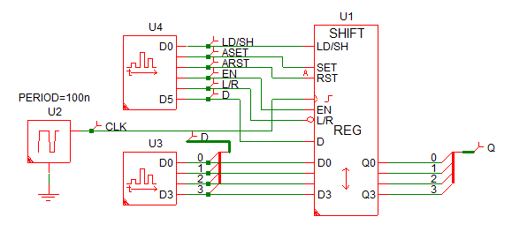
This example of the shift register uses two Digital Signal Sources to generate the input pulses to the shift register. The input source waveforms are defined in a text file with each state transition defined on a single line. These two sources excite every state transition in the truth table. The example uses asynchronous set/reset.
For clarity, the simulation waveforms taken from the circuit example have been divided into three sections.
The image below shows the Load and Shift behavior when the D input is 0. During a Left shift operation, the D input is shifted into the LSB, and since D=0, the new Q output is twice the old Q. For a Right shift the D input is shifted into the MSB, and since D=0, the new Q output is half the old Q. The initial condition of the Shift Register is set to 15 decimal in the example.
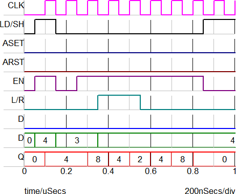
| Time | Event | Q Output |
100n |
Load | 4 |
200n |
Retain state | 4 |
300n |
Shift left | 8 |
400n |
Shift right | 4 |
500n |
Shift right | 2 |
600n |
Shift left | 4 |
700n |
Shift left | 8 |
800n |
Shift left | 0 |
The image below shows the Load and Shift behavior when the D input is 1. During a Left shift operation, the D input is shifted into the LSB, effectively adding one to the result. For a Right shift the D input is shifted into the MSB, adding 2n-1 to the result. For this example, n=4, so the MSB is equal to 8.
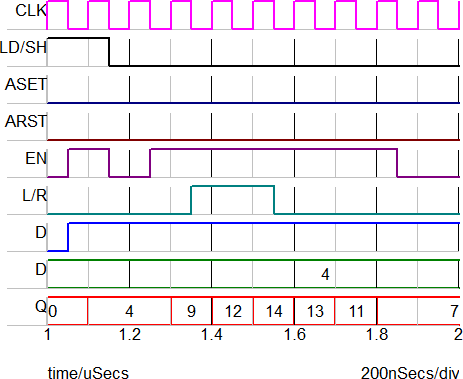
| Time | Event | Q Output |
1.1u |
Load | 4 |
1.2u |
Retain state | 4 |
1.3u |
Shift left | 9 |
1.4u |
Shift right | 12 |
1.5u |
Shift right | 14 |
1.6u |
Shift left | 13 |
1.7u |
Shift left | 11 |
1.8u |
Shift left | 7 |
The image below shows the set/reset behavior of the register.
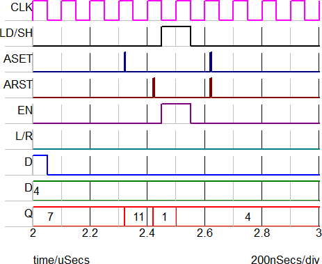
| Time | Event | Q Output |
2.32u |
Asynchronous set | 11 |
2.42u |
Asynchronous reset | 1 |
2.5u |
Load | 4 |
2.62u |
Illegal concurrent ASET and ARST | 4 |
Because the shift register model is generated by a template script when the simulation is executed, a fixed model cannot be inserted into a netlist. The template script for this device is simplis_make_register_model.sxscr, which you, as a licensed user, can download in a zip archive of all built-in scripts.
To download this zip file, follow these steps:
Note: You will be prompted to log in with the user name and password given to you when you registered.