5.2 Set up a Load Transient Simulation
In the previous section you added a compensator to the power stage, closing the control loop. The AC response of the converter shows adequate small-signal stability in terms of gain and phase margin. The next step is to verify the large-signal stability in the time domain when a load transient is applied to the converter output.
In this topic:
Key Concepts
- SIMPLIS runs the three simulations (POP, AC, and Transient) in that order, which means that the transient simulation begins with the converter in steady state.
- When a transient simulation is run after a POP simulation:
- Only the transient data is shown on the waveform viewer.
- The transient simulation starts at the last data point from the POP simulation; that is, the POP simulation determines the initial conditions for the transient simulation.
- During a POP simulation, the pulse current source is held at its initial value of 0A.
What You Will Learn
- How to configure the circuit for a load transient test using a pulse current source.
- How the POP trigger conditions affect the initial conditions for the transient analysis.
5.2.1 Add a Pulse Current Source
To set up the load transient simulation, you will add a pulse current source in parallel with the load resistor and change the output load resistor value.
- The converter will be set to start with a 50% load (5A) provided by the load resistor; the current source will apply a 0-5A load pulse.
- The load timing will be set to apply a worst-case pulse load for this trailing edge modulator.
- The worst case pulse load timing conditions are as follows:
- The step-up occurs when the PWM modulator turns off the high side MOSFET.
- The step-down occurs when the PWM modulator turns the MOSFET on.
- The timing for the load transient can be set precisely during a POP/Transient analysis.
To get started, you will need the schematic from the last section. You can download a schematic at this stage here: 11_SIMPLIS_tutorial_buck_converter.sxsch.
To add the pulse current source, follow these steps:
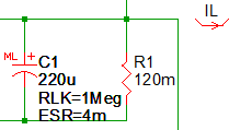
- Select the inline current probe (IL); press Ctrl+C to make a copy; and
then press Ctrl+V to paste the current probe to the right of the load resistor
R1 as shown below.
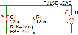
- Double click on the probe, and rename the probe PULSE LOAD.
- In the part selector, double click on the Current Sources category to expand the list.
- Double click on Waveform Generator - Current Source and place that symbol to the
right of the load resistor and the PULSE LOAD probe; and then wire it to the load
resistor and current probe as shown below:
To edit the waveform generator parameters, follow these steps:
- Double-click on I1.
- On the right side of the dialog in the Wave Shape section, select the One pulse radio button.
- In the left column, change Delay to 10.22u. Note: This delay time is equal to 5 switching periods plus a single on-time of the MOSFET.Result: This will delay the start of the load pulse until right after the switch turns off, producing the worst-case load transient.
- In the first column near the top of the dialog, change Width to 29.68u.
Result: The Width, when added to the Delay and Rise parameters, will delay the load step-down time to 40us.
- Uncheck Default rise and fall .
- In the Rise field, enter 100n for the rise time.Result: The fall time is automatically set to 100n. The Edit Waveform dialog should now look like this:
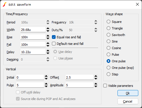
- Click Ok to save the new parameter values.
- Double click on the load resistor R1, and change the value to 240m.
5.2.2 Set up Analysis Parameters
Now that you have configured the schematic for the pulse load test, you are ready to set the analysis parameters to run a POP and transient simulation. The stop time for this simulation is set to 70us, which is long enough to for the converter to recover from the load transient and enter steady-state.
To set the analysis parameters, follow these steps:
- From the menu bar in the Schematic editor, select .
- Uncheck AC, and check Transient.
- Click the Transient tab.
- In the Analysis parameters section, set the Stop time to 70u.Result: The Transient tab should now look like this:
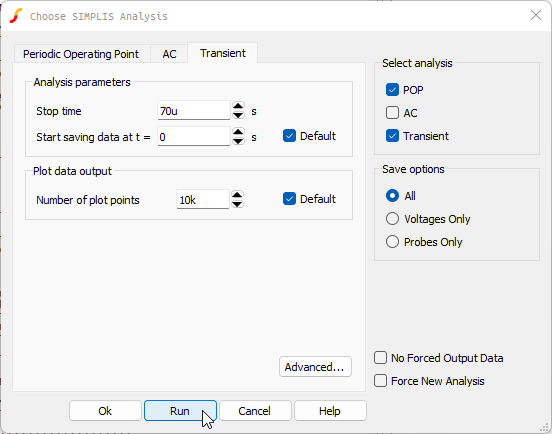
- To run the POP/Transient simulation, click Run button.Result: SIMPLIS runs POP and Transient simulations. After the POP simulation, SIMPLIS takes the initial conditions of the circuit and applies them to the Transient simulation. The Transient simulation starts with the converter in steady-state.
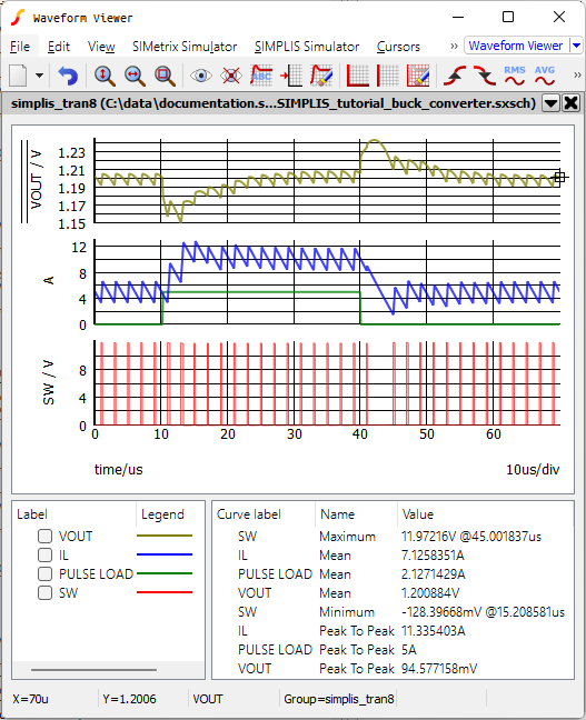
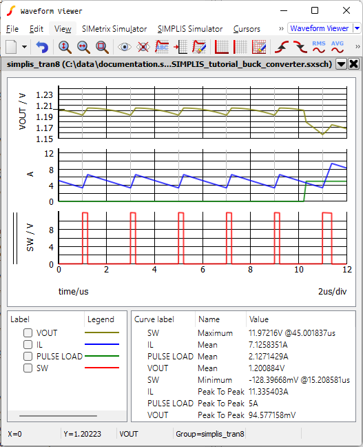
If you look closely at the waveforms, you will notice that the timing appears to be incorrect. While the pulse load starts rising after the delay time of 10.22μs as setup in the previous section, the power stage waveforms are time-shifted by approximately 1μs, or half the period. Below is the waveform viewer zoomed in on the first 12μs:
The POP trigger conditions are the reason for this apparent time shift. In 5.1 Building a Compensator, you moved the POP trigger gate from the switching node to the oscillator source. The POP analysis settings include an edge direction, and the default setting is to trigger on the rising edge. Since the POP Trigger is finding the 500mV level of the rising edge of the oscillator sawtooth ramp, the POP period starts at a time midway between the switching node rising edge. Since the transient analysis begins at the final time point from the POP analysis, there is a 1μs time shift in the transient waveforms. In the next section you will change the POP Trigger Edge and see the effect on the transient waveforms.
5.2.3 Change POP Trigger Edge
To change the POP trigger edge, follow these steps:
- From the menu bar in the Schematic editor, select .
- Click on the POP Tab and then select the Falling edge (logic high to logic low)
radio button.Result: The dialog should appear as follows:
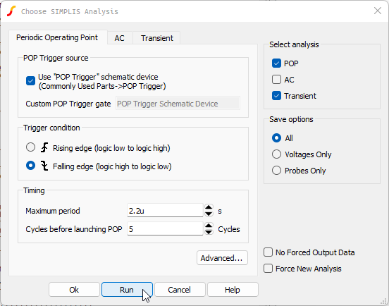
- Click Run to rerun the POP/Transient simulation.Result: The simulation runs again, but with a falling edge POP trigger condition. Because the POP Trigger condition is set to the oscillator falling edge, the MOSFET turns on slightly after t=0, t=2μs, t=4μs, etc. The timing of the pulse load is now aligned with the expected switching period and, therefore, the worst-case load transient timing conditions are used.
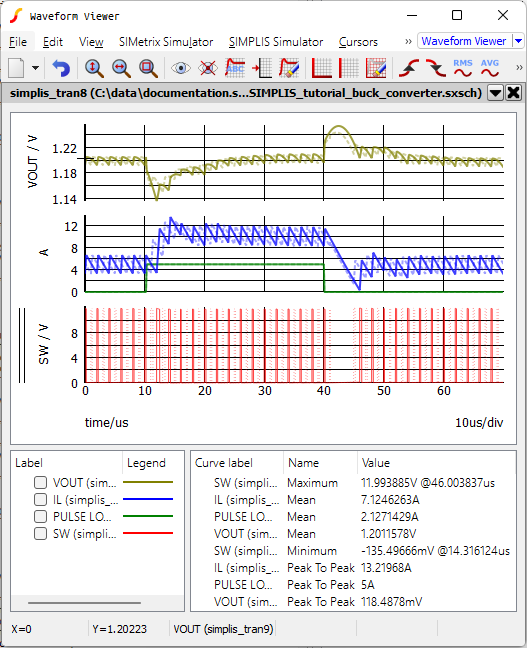
It is now obvious how the output voltage deviation from steady-state is affected by the timing of the load pulse. The first simulation applied the pulse approximately 1us later (or earlier) in the switching period than the desired worst-case conditions.
5.2.4 Add the AC analysis to the POP/Transient Simulation
In the previous section, you set up the converter to run a POP and Transient simulation. This was done for clarity because a single graph tab with the transient results is output for each simulation. You can run an AC simulation in combination with both the POP and transient simulations. SIMPLIS will run the resulting POP/AC/Transient simulations in that order.
Running a POP/AC/Transient simulation allows you to examine both the large- and small-signal behavior of the circuit.
To add the AC analysis and view both types of behavior, follow these steps:
- From the menu bar in the Schematic editor, select .
- In the Select analyses section on the right, check AC.
- At the bottom of the dialog, click Run.Result: The waveform viewer opens with two tabs: an AC tab and a transient tab. The transient tab shows the large-signal behavior.
- To view the small-signal behavior, click on the AC tab.
5.2.5 Save your Schematic
To save your schematic, follow these steps:
- Click anywhere in the schematic to bring the schematic viewer in to focus.
- Select .
- Navigate to your working directory where you are saving your schematics.
- Name the file 12_my_buck_converter.sxsch.