Arbitrary Logic Block - User Defined Models
In this topic:
Overview
The arbitrary logic block is an internal component that can be defined to perform any logic function. Using a simple descriptive language it is possible to define combinational logic elements, synchronous and asynchronous registers as well as look-up table (ROMs) and arrays (RAMs).
Each ALB device is defined as a normal .MODEL statement which refers to a separate file containing the logic description. This section is mostly concerned with the descriptive language used in the definition file.
An Example
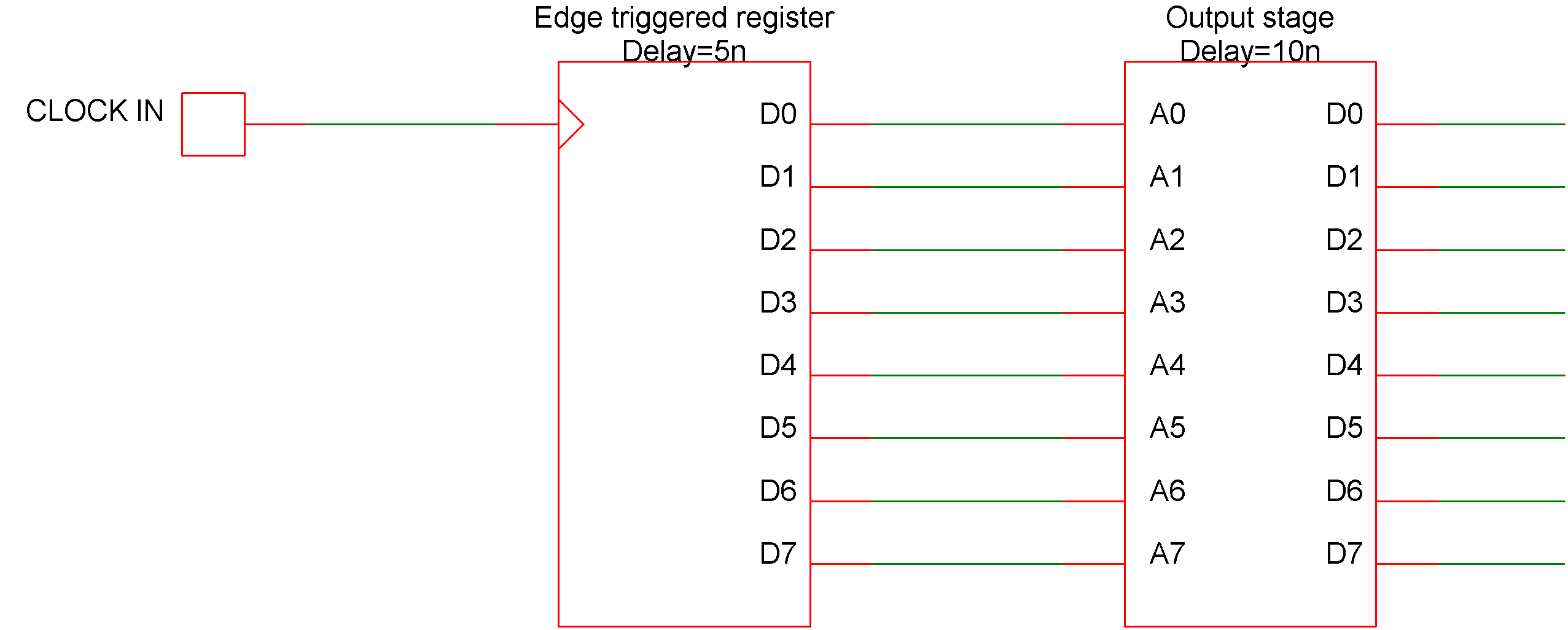
We start with a simple example. The following is a description of a simple 8 bit synchronous counter. (This definition would be put into a file referred to in a .MODEL statement. This is described later). A circuit using this model is supplied as an example. See EXAMPLES/ALB_Examples/count.sch
PORT (DELAY = 10n) CountOut out[0:7] ;
EDGE (DELAY=5n, WIDTH=8, CLOCK=in[0]) Count ;
Count = Count + 1 ;
CountOut = count ;
We will go through this line by line.
PORT (DELAY = 10n) CountOut out[0:7] ;
(DELAY = 10n)
says that the output delay is 10nS that is the actual output pins will change state 10nS after the output is assigned.
CountOut
names the output CountOut.
out[0:7]
defines the port as an output and specifies the actual pins used on the device. This specifies the first 8 pins on the output port. There are two sets of pins on an ALB one assigned for inputs and referred to as "in[a:b]" and the other assigned for outputs and referred to as "out[a:b]". The line ends in a semi-colon which terminates the statement. All statements must end in a semi-colon.
The next line:
EDGE (DELAY=5n, WIDTH=8, CLOCK=in[0]) Count ;
defines an edge triggered register.
CLOCK=in[0]
specifies the pin used for the clock (it must always be an input pin). This is always positive edge triggered.
DELAY=5n
This is the clock to output delay. (See illustration below)
WIDTH=8
This specifies the width of the register i.e. 8 bits
The next line:
Count = Count + 1 ;
defines the operation to be performed at each clock edge. In this case the value in the register is simply incremented by one. When it reaches 255 it will reset to 0.
The final line
CountOut = count ;
defines what appears at the output. This says that the output equals the count register.
The following diagram illustrates the internal structure of the counter.
Reset Count at 200
We will now make a small modification to the counter so that the counter only counts up to 199 before resetting back to zero. Change the line:
Count = Count + 1 ;
to:
Count = Count==199 ? 0 : Count + 1 ;
This says 'If the count equals 199 set to zero otherwise increment by one'. As before, this will happen on each clock edge.
Add an Asynchronous Reset
The logic definition language supports the addition of asynchronous controls to synchronous registers. Here we will add an asynchronous reset. The complete definition becomes:
PORT   (DELAY = 10n)   CountOut   out[0:7] ;
PORT                   Reset      in[1] ;

EDGE (DELAY=5n, WIDTH=8, CLOCK=in[0]) Count ;

Count := !Reset ? 0 ;
Count = Count==199 ? 0 : Count + 1 ;

CountOut = count ;
To add the reset signal we have to add two lines to the definition. The first:
PORT Reset in[1] ;
defines the signal pin to be used for the reset and the second:
Count := !Reset ? 0 ;
defines the action to be taken. This is an asynchronous action statement. The '!' means NOT so the line says 'If Reset is NOT TRUE (i.e. low) set the count to zero otherwise do nothing'. Asynchronous action statements are always of the form:
register_name := condition ? action ;
The ':' signifies that the statement is asynchronous and that the action should happen immediately.
Example 2 - A Simple Multiplier
PORT (DELAY=10n) MultOut out[0:7] ;
PORT in1 in[0:3] ;
PORT in2 in[4:7] ;

MultOut = in1*in2 ;
The above defines a simple combinational circuit, that of a 4X4 digital multiplier. The inputs in1 and in2 are treated as 4 bit unsigned values so if both are zero the output will be zero and if both are 1111 (i.e. 15) the result will be 11100001 (i.e. 225). See the circuit EXAMPLES/ALB_Examples/Mult.sch.
Example 3 - A ROM Lookup Table
The following definition is that of a lookup table to define a sine wave:
PORT (DELAY=10n) ROMout out[0:7] ;
PORT             input in[0:7] ;

READONLY (WIDTH=8) ROM[256] =

128, 131, 134, 137, 140, 143, 146, 149, 152, 156, 159, 162,
165, 168, 171, 174, 176, 179, 182, 185, 188, 191, 193, 196,
199, 201, 204, 206, 209, 211, 213, 216, 218, 220, 222, 224,
226, 228, 230, 232, 234, 236, 237, 239, 240, 242, 243, 245,
246, 247, 248, 249, 250, 251, 252, 252, 253, 254, 254, 255,
255, 255, 255, 255, 255, 255, 255, 255, 255, 255, 254, 254,
253, 252, 252, 251, 250, 249, 248, 247, 246, 245, 243, 242,
240, 239, 237, 236, 234, 232, 230, 228, 226, 224, 222, 220,
218, 216, 213, 211, 209, 206, 204, 201, 199, 196, 193, 191,
188, 185, 182, 179, 176, 174, 171, 168, 165, 162, 159, 156,
152, 149, 146, 143, 140, 137, 134, 131, 128, 124, 121, 118,
115, 112, 109, 106, 103, 99, 96, 93, 90, 87, 84, 81, 79, 76,
73, 70, 67, 64, 62, 59, 56, 54, 51, 49, 46, 44, 42, 39, 37,
35, 33, 31, 29, 27, 25, 23, 21, 19, 18, 16, 15, 13, 12, 10,
9, 8, 7, 6, 5, 4, 3, 3, 2, 1, 1, 0, 0, 0, 0, 0, 0, 0, 0, 0,
0, 0, 1, 1, 2, 3, 3, 4, 5, 6, 7, 8, 9, 10, 12, 13, 15, 16,
18, 19, 21, 23, 25, 27, 29, 31, 33, 35, 37, 39, 42, 44, 46,
49, 51, 54, 56, 59, 62, 64, 67, 70, 73, 76, 79, 81, 84, 87,
90, 93, 96, 99, 103, 106, 109, 112, 115, 118, 121, 124 ;

ROMout = ROM[input] ;
See the example circuit EXAMPLES/ALB_Examples/SineLookUp.sch
Example 4 - D Type Flip Flop
The following is the definition for the 74X74 Dtype flip flop supplied with the standard SIMetrix model library. This model is somewhat more complicated as it models a number of timing artefacts such as setup time and minimum clock width. Each line below has been annotated to describe its function. Full details are explained in the following sections.
// Input port definitions
PORT D    in[0] ;    // D input
PORT CK   in[1] ;    // Clock
PORT SR   in[2:3] ;  // Set/reset inputs. r bit 3 s bit 2

PORT out  out[0:1] ; // Outputs Q and !Q

// Edge triggered register.
// HOLD is hold time i.e. time after clock edge that data
// must remain stable. Setup time is implemented by
// delaying the D input

// MINCLOCK is minimum clock width.
// USER[n] references values supplied in the .MODEL statement
// The final '=2' initialise the register with the value 2
// i.e. Q=0 and Q!=1
EDGE (WIDTH=2, DELAY=USER[4], HOLD=USER[2], MINCLOCK=USER[3],
CLOCK=in[1]) DTYPE=2;

// COMB defines a combinational register. This is effectively
// a delay element. These delay the D input (to implement
// setup time) and the set/reset inputs to implement minimum
// set and reset times
COMB (DELAY=USER[0], WIDTH=1) D_DEL ;
COMB (DELAY=USER[1], WIDTH=2) SR_DEL ;

// These assign the combinational registers
SR_DEL = SR ;
D_DEL = D ;

// asynchronous action
DTYPE := SR_DEL==1||SR_DEL==2 ? (SR_DEL==2 ? 1 : 2) ;

// synchronous action
DTYPE = D_DEL ? 1 : 2 ;

// Both outputs are forced high if S and R are both active
// Output will be restored to previous value when one of
// S and R becomes inactive
out = SR_DEL==0 ? 3 : DTYPE ;
Device Definition - Netlist Entry and .MODEL Parameters
Netlist entry
Axxxx [ in_0 in_1 .. in_n ] [ out_0 out_1 .. out_n ] model_name
+ : parameters
Connection details
| Name | Description | Flow | Type |
| in | Input | in | d |
| out | Output | out | d |
Instance parameters
| Name | Description | Type |
| trace_file | Trace file | string |
| user | User device parameters | real vector |
Model format
.MODEL model_name d_logic_block parameters
Model parameters
| Name | Description | Type | Default | Limits | Vector bounds |
| file | Definition file name | string | none | none | n/a |
| def | Definition | string | none | none | n/a |
| out_delay | Default output delay | real | 1n | ???MATH???1\text{e}^{-12} - \infty???MATH??? | n/a |
| reg_delay | Default internal register delay | real | 1n | ???MATH???0 - \infty???MATH??? | n/a |
| setup_time | Default level triggered setup time | real | 0 | ???MATH???0 - \infty???MATH??? | n/a |
| hold_time | Default edge triggered hold time | real | 0 | ???MATH???0 - \infty???MATH??? | n/a |
| min_clock | Default minimum clock width | real | 0 | ???MATH???0 - \infty???MATH??? | n/a |
| trace_file | Trace log file | string | none | n/a | |
| user | User defined parameters | real vector | none | none | none |
| user_scale | Scale of user values | real | 1 | ???MATH???0 - \infty???MATH??? | n/a |
| input_load | Input load value (F) | real | 1p | none | n/a |
| family | Logic family | string | UNIV | none | n/a |
| in_family | Input logic family | string | UNIV | none | n/a |
| out_family | Output logic family | string | UNIV | none | n/a |
| out_res | Digital output resistance | real | 100 | ???MATH???0 - \infty???MATH??? | n/a |
| min_sink | Minimum sink current | real | -0.001 | none | n/a |
| max_source | Maximum source current | real | 0.001 | none | n/a |
| sink_current | Input sink current | real | 0 | none | n/a |
| source_current | Input source current | real | 0 | none | n/a |
Notes
Usually the logic block definition would be placed in a file referred in the FILE parameter. Alternatively the definition may be placed directly in the .MODEL statement as the value of the DEF parameter. In this case the definition must be enclosed in quotation marks (").
The USER_SCALE parameter scales all values found in the USER parameter.
Language Definition - Overview
The following sections describe the full details of the arbitrary logic block language.
All logic definitions are divided into two sections. The first contains the ports and register definitions and the second section consists of the assignment statements. (The first section can be empty in very simple cases).
Language Definition - Constants and Names
Constants follow the usual rules. Any decimal number with optional sign and exponent or engineering suffix is permitted. In addition, numbers in hexadecimal are also allowed. The format is the same as for the 'C' programming language i.e. prefixed with '0X'. E.g.:
0X10 = 10 hex = 16.
Identifiers used for register, port and variable names must begin with an alphabetic character or underscore and consist of alphanumeric characters and underscores.
Language Definition - Ports
Port statements define the inputs and outputs to the logic device. They are of the form
PORT ( DELAY=output_delay) port_name OUT [ pin1| pin1:pin2 ]
OR
PORT port_name IN|OUT [ pin1| pin1:pin2 ]
Ports define a label to a single pin or sequence of pins so that they can be treated as a single entity in the remainder of the logic definition. In the case of outputs they can optionally also define an output delay. (If this is not specified a default output delay defined in the devices .MODEL statement is used).
| port_name | Any name to reference the port. Must start with a letter or underscore and consist only of letters numbers and underscores. Names are not case sensitive. |
| pin1,pin2 | Identifies pin or range of pins that port accesses. See next section for more details. |
| output_delay | Output delay in seconds. When an output port is assigned a value, the actual output is updated after this delay has elapsed (+ any loading delay). You may use engineering units in the normal way. E.g. 10n is 10e-9. |
Relationship between ports, netlist entry and symbol definition
The netlist entry for an arbitrary logic block is of the form:
Axxx [ input_node_list ] [ output_node_list ] model_name
The pin numbers in the port statements above, i.e. pin1 and pin2 are the positions within the input_node_list for input ports and output_node_list for output ports.
So if the netlist entry is:
A12 [ 1 2 3 4 ] [ A B C D ] ARB1
the port definition:
PORT output OUT[0:3] ;
assigns the label output to the netlist pins A B C and D. If, for example, the value 7 is evaluated and assigned to output, pins A B and C would be set to a logic '1' and pin D would be set to a logic '0'. Pins 1 2 3 & 4 would be used for input ports in a similar way.
The netlist entry relates directly to a symbol definition for an arbitrary logic block. When defining a symbol to be used with an ALB you should observe the following rules
- The first input pin's name and the first output pin's name should both be prefixed with a '['.
- The last input pin's name and the last output pin's name should both be suffixed with a ']'.
- Use to define the pin order with input pins first then output pins.
- You should assign a MODEL property with the value 'A'.
Language Definition - Registers and Variables
Registers are the main working elements of the arbitrary logic block. There are four main types. These are:
- Edge triggered. The value of these change on the rising edge of an assigned clock.
- Level triggered. The value of these change when an assigned enable is at a logic '1' level.
- Combinational. The value of these change after a specified delay.
- Read-only. These are given a fixed value which cannot be changed. These would usually be arranged in indexable arrays to implement a read only memory.
In addition to registers there are also local variables. These can be assigned a value that can later be used in a register assignment.
All registers must be declared. Local variables are declared by simply assigning a value to them.
The syntax for register declarations follow:
Edge Triggered Register Declaration
EDGE ( CLOCK=input_pin_spec
[, DELAY=reg_delay]
[, WIDTH=reg_width]
[, MINCLOCK=reg_minclock]
[, HOLD=reg_hold_time]
[, ASYNCDELAY=reg_asyncdelay]
[, BITWISE=0|1 ] ) name [[array_size]]
[ = initial_condition *[, initial_condition] ] ;
| input_pin_spec | This specifies which input pin is the clock and must be of the form: IN[n] where n is a pin number. See Relationship between ports, netlist entry and symbol definition for details on how pin numbers relate to netlist entries and symbol definitions. |
| reg_delay | Register delay in seconds. This is the delay between the clock rising edge and the register value changing. You can use engineering units in the normal way. Default: REG_DELAY parameter in .MODEL statement defines default value. This is turn has a default value of 1nS. |
| reg_width | Register width in bits. This has a maximum of 32. Default: 32 |
| reg_minclock | Minimum clock width. This must be less than or equal to reg_delay. The register value will not update if the clock width is less than this value. Default: MIN_CLOCK parameter in .MODEL statement defines default value. This in turn has a default value of 0. |
| reg_hold_time | Register hold time. This is the time that the input data (i.e. assignment value) must remain stable after the clock edge, for the new value to be accepted. If the BITWISE parameter is set to '1' (which it is by default) the hold time is applied on a bit by bit basis. That is any individual bit in the register that remains stable during the hold period will attain the new value even if other bits violate the hold time. If BITWISE is '0' then if a single bit violates the hold time, the whole register will remain unchanged even if some bits remain stable during the hold period. Setting BITWISE to '0' saves system memory which can be important for large arrays (i.e. RAMs). Default: HOLD_TIME parameter in .MODEL statement defines default value. This in turn has a default of 0. |
| reg_asysncdelay | Time the register takes to acquire a value set by an asynchronous assignment. This must be less than or equal to reg_delay. Default: reg_delay |
| BITWISE value | See reg_hold_time Default: '1' for single registers, '0' for arrays. |
| name | Register name. |
| array_size | If specified, the register is arranged as an addressable array of size array_size. Default: 1 |
| initial_condition | Value assigned to register when simulation starts. Default: 0 |
Level Triggered Register Declaration
LEVEL (CLOCK=input_pin_spec
[, DELAY=reg_delay]
[, WIDTH=reg_width]
[, SETUP=reg_setup_time]
[, ASYNCDELAY=reg_asyncdelay]
[, BITWISE=0|1 ]  name [[array_size]]
[ = initial_condition  *[, initial_condition]] ;
| input_pin_spec | This specifies which input pin is the enable and must be of the form: IN[n] where n is a pin number. See Relationship between ports, netlist entry and symbol definition for details on how pin numbers relate to netlist entries and symbol definitions. |
| reg_delay | Register delay in seconds. If the enable is already high, this is the time taken for the register to acquire new data. Otherwise it is the delay between enable rising edge and the register value changing. You can use engineering units in the normal way. Default: REG_DELAY parameter in .MODEL statement defines default value. This is turn has a default value of 1nS. |
| reg_width | Register width in bits. This has a maximum of 32. Default: 32 |
| reg_setup_time | Register hold time. This is the time that the input data (i.e. assignment value) must remain stable prior to an enable falling edge, for the new value to be accepted. If the BITWISE parameter is set to '1' (which it is by default) the setup time is applied on a bit by bit basis. That is any individual bit in the register that remains stable during the setup period will attain the new value even if other bits violate the setup time. If BITWISE is '0' then if a single bit violates the setup time, the whole register will remain unchanged even if some bits remain stable during the setup period. Setting BITWISE to '0' saves system memory which can be important for large arrays (i.e. RAMs). Default: SETUP_TIME parameter in .MODEL statement defines default value. This in turn has a default of 0. |
| reg_asysncdelay | Time the register takes to acquire a value set by an asynchronous assignment. This must be less than or equal to reg_delay. Default: reg_delay |
| BITWISE value | See reg_setup_time Default: '1' for single registers, '0' for arrays. |
| name | Register name. |
| array_size | If specified, the register is arranged as an addressable array of size array_size. Default: 1 |
| initial_condition | Value assigned to register when simulation starts. Default: 0 |
Combinational Register Declaration
COMB ( [, DELAY=reg_delay]
[, WIDTH=reg_width]
[, BITWISE=0|1 ] ) name [ = initial_condition ] ;
| reg_delay | Register delay in seconds. You can use engineering units in the normal way. If BITWISE is '1' (the default) this delay is applied on a bit by bit basis. If BITWISE is '0' then the delay is applied to the whole register. That is the output will not change until all inputs have remained stable for the delay time. Setting BITWISE to '0' is useful when using combinational registers to implement asynchronous state machines as it eliminates race conditions. Default: REG_DELAY parameter in .MODEL statement defines default value. This is turn has a default value of 1nS. |
| reg_width | Register width in bits. This has a maximum of 32. Default: 32 |
| name | Register name. |
| initial_condition | Value assigned to register when simulation starts. Default: 0 |
Read-only Register Declaration
READONLY ([, WIDTH=reg_width]  name[[array_size]]
[ = initial_condition  *[, initial_condition]] ;
| reg_width | Register width in bits. This has a maximum of 32. Default: 32 |
| array_size | If specified, the register is arranged as an addressable array of size array_size. Default: 1 |
| name | Register name. |
| initial_condition | Value assigned to register when simulation starts. Default: 0 |
Language Definition - Assignments
Registers and output ports can be assigned using the assignment operator '='. Assignment values can be constants, input ports, other registers, local variables or expressions of any or all of these. Assignments are of the form:
register | output_port | OUT[pin1:pin2] | OUT[pin1] | local_var = expr ;
OR
clocked_register[index] = expr ;
| register | Combinational, edge triggered or level triggered register name. |
| output_port | Output port name |
| pin1, pin2 | Output pin numbers. OUT[pin1:pin2] and OUT[pin1] allow outputs to be assigned with having to declare them in a PORT statement. |
| local_var | Any name not already used for a port or register. This defines the value for a local variable that can be used in subsequent expressions. A local variable may not be used in an expression that precedes its definition. |
| expr | Local variables, input ports, registers and constant values combined using arithmetic, Boolean, bitwise Boolean, shift, conditional and relational operators. See Expression Operators for detailed documentation on all operators. |
| clocked_register | Edge or level triggered register. |
| index | Array index. This must be smaller than the array size. Arrays are based at 0. That is the first element is zero and the last is (array length-1). |
Expression operators
The following table lists all operators available. These are listed in order of precedence. Precedence determines the order of evaluation. For example in the expression:
var1<var2 && var3<var4
The sub-expressions var1<var2 and var3<var4 are evaluated first and the result of that those evaluations combined using && to yield the final result. This is because < has higher precedence than &&. The precedence can be altered using parentheses in the usual way.
| Class | Operators | Description |
| Index | [] | E.g. var1[4]. Index operator to access array element. |
| Unary | + - | Operator to single value e.g. -5 |
| Arithmetic multiplicative | * / % | Arithmetic multiply/divide/modulus treating all values as unsigned integers. % returns remainder after division |
| Arithmetic additive | + - | Arithmetic operation treating all values as unsigned integers |
| Shift | << >> | Shift-left and shift right. E.g. reg1 << 2 will shift reg1 left by two bits |
| Relational | < > <= >= | If condition met result is 1 (=TRUE) otherwise result is zero (=FALSE) |
| Equality | == <> != | == means EQUAL <> and != both mean NOT EQUAL Return 1 when condition met and 0 when condition is not met |
| Bitwise AND | & | Performs a Boolean AND bit by bit |
| Bitwise XOR | ^ | Performs a Boolean exclusive OR bit by bit |
| Bitwise OR | | | Performs a Boolean OR bit by bit |
| Logical AND | && | Returns 1 if both values are non-zero (TRUE) otherwise returns zero (FALSE) |
| Logical OR | || | Returns 1 if either value is non-zero (TRUE) otherwise return zero (FALSE) |
| Conditional expression | cond ? res1 : res2 | Returns res1 if cond is non-zero (TRUE) otherwise returns res2 Example A<B ? 16 : 0 returns 16 if A is less than B otherwise returns 0 |
Controlling Output Enables
An output can be set into a high impedance state using a modification to an output port variable. Use the suffix .EN after the output port or port identifier to signify that the result of the expression should control the output enable. E.g. the following is extracted from the 74XX244 definition:
PORT (DELAY=USER[0]) Output out[0:3] ;
Output.En = Out_En_Del ? 0 : 0xf ;
Examples
Y = !Enable ? A_Del != B_Del : 1 ;
If Enable is 0 then Y will be the result of A_Del != B_Del otherwise the result will be 1.
Shift = !Par_En_Del ? Par_Data_Del :(Shift<<1) | Ser_Data_Del;
This describes the action of a parallel loadable shift register.
out[0]= !in[1]&!in[2] | in[1]&!in[2]&in[0] |
!in[1]&in[2]&in[0]
An example of referencing inputs and outputs directly without needing PORT statements.
Language Definition - User and Device Values
Sometimes it is convenient to use the logic description to define the functionality of a block but have the timing and other specifications specified separately. This is achieved by USER and DEVICE values. USER values are specified in the .MODEL statement while DEVICE values are specified on the device at the netlist (or schematic device) level. The values are referenced in the logic definition in the form:
USER[index]
and
DEVICE[index]
These can replace any constant value in an expression, register qualifier or port qualifier. (Register and port qualifiers are the values in parentheses after the register/port keyword. E.g. DELAY, HOLD, SETUP etc.).
To set USER values in a .MODEL statement, assign the parameter USER. This is a vector parameter, that is it can have any number of values and these must be enclosed in square brackets '[' and ']'. For example:
.MODEL Counter8 d_logic_block file=counter_8.ldf
+ user=[10n, 5n]
The logic definition to which this model refers - counter_8.ldf - can use USER[0] and USER[1] to refer to the values 10n and 5n respectively.
To set DEVICE values in a netlist, the netlist entry for the device must be appended with:
: USER=[ values ]
For example:
A$U3 [clock] [Q0 Q1 Q2 Q3 Q4 Q5 Q6 Q7] Counter8 :
+ USER=[10n, 5n]
The logic definition for this device can use DEVICE[0] and DEVICE[1] to access the USER values in the netlist i.e. 10n and 5n respectively. Always remember to include the colon. This acts as a separator between the device name and any parameters.
Diagnostics: Trace File
In order to debug models, a tracing facility is provided. If the .MODEL TRACE_FILE parameter or instance parameter of the same name is specified, a file will be created which lists the values of all internal registers at each time point.
The file will usually have a number of lines of the form: Roll back to <time>
5.00022e-05    2696     9    2696    0
5.09397e-05    2696     9    2696    0
5.09407e-05    2692     10   2692    0

Roll back to 5.08599e-05

5.09397e-05    2696     9    2696    0
5.09407e-05    2692     10   2692    0
5.09657e-05    2692     10   2692    0
Roll-back occurs when an analog time step is rejected but the digital simulation has already advanced past the new analog time. In this case the digital simulator has to back-track events. This mechanism is central to the operation of the mixed-mode system and is explained in more detail in Mixed-mode Simulator - How it Works.
| ◄ Digital Model Libraries | Mixed-mode Simulator - How it Works ▶ |