Example 5 -- Regulated Converter
The diagram shown in fig. 9.13 is the schematic of a regulated current step-up (buck) converter operating under a fixed-frequency control law.
The modeling of the switching transistor, the diode, the energy-storage inductor, the output-filter capacitor, and the load of the power stage is similar to the modeling of the corresponding components in Example 4 and is not elaborated on here. Again, with the transistor modeled as a simple controlled switch, the base-drive shown in 9.13 does not need to be modeled in the input file as the output of the comparator can directly control the simple transistor switch.
The error amplifier in the controller is shown separately in 9.14 (a) and its piecewise-linear equivalent is shown in 9.14 (b). The operational amplifier is modeled with an input resistance RIN between its differential inputs and the voltage- controlled voltage source EOP at its output. 9.14 illustrates how an opamp circuit can be modeled by a simple network if the opamp is not driven into saturation. More sophisticated models for the operational amplifier can be built upon this basic model.
The input file describing this converter is shown in 9.15. In this example, we are interested in the steady-state waveforms of the sawtooth voltage V(11), the voltage V(RL) across the load and the current I(L) through the inductor.
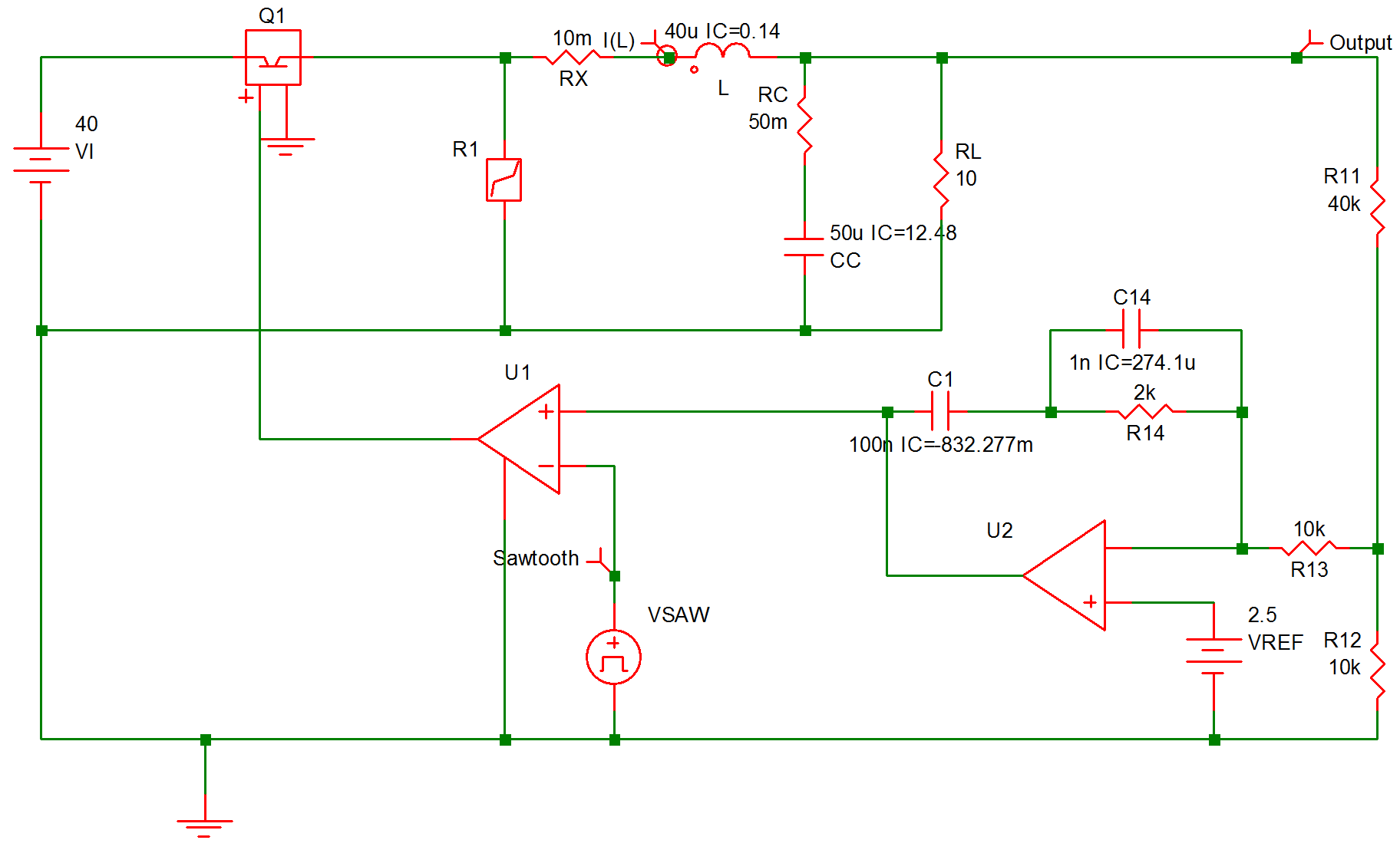 |
9.13 Example 5 Regulated Converter |
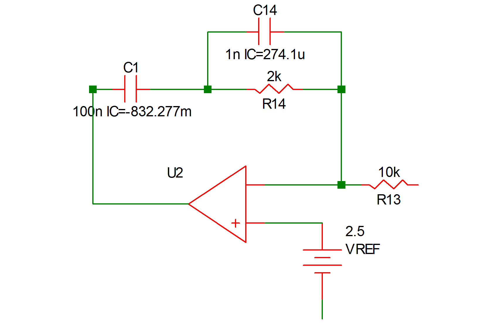 |
9.14a Error Amplifier Circuit |
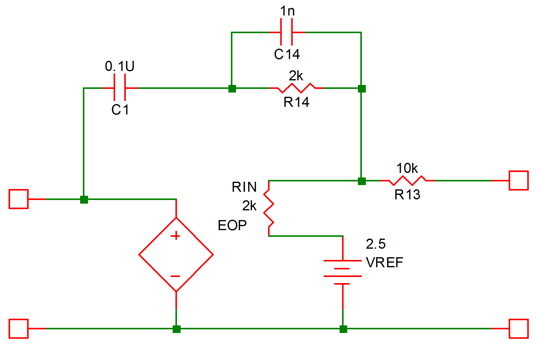 |
9.14b Piecewise-linear Equivalent |
* Regulated Converter
.PRINT  ALL
.OPTIONS  PSP_NPT=201
.TRAN 50u 0
X$U2 11 13 10 opamp
VSAW 12 0 SAW V1=0 V2=5 FREQ=100k DELAY=0 OFF_UNTIL_DELAY=NO
X$U1 6 0 11 12 SIMPLIS_COMP$1
VREF 13 0 2.5
L 4 5 40u IC=0.14
VI 2 0 40
R12 0 8 10k
R13 8 10 10k
RC 7 5 50m
RL 5 0 10
R11 8 5 40k
C1 11 9 100n IC=-832.277m
R14 10 9 2k
C14 9 10 1n IC=274.1u
CC 7 0 50u IC=12.48
Q1 2 3 6 0 Q1$TP_VCQ IC=OPEN
.MODEL Q1$TP_VCQ VCQPOS VSAT=700m RSAT=100m ROFF=10Meg
+ GAIN=10 TH=2.5 HYSTWD=100u LOGIC=POS LEVEL=1
!R$R1 0 3 R1$TP_SSPWLR IC=1
.MODEL R1$TP_SSPWLR VPWLR NSEG=2 X0=0 Y0=0 X1=0.7 Y1=10U
+ X2=0.8 Y2=1.00001
RX 4 3 10m
.SUBCKT SIMPLIS_COMP$1  201 100 101 102
!DCOMP 201 100 101 102 MCOMP IC=1
.MODEL MCOMP COMP RIN=1e+007 ROUT=50 VOL=0 VOH=5
+ HYSTWD=1e-006 DELAY=0
.ENDS SIMPLIS_COMP$1
.SUBCKT opamp  2 3 1
.NODE_MAP VINN 1
.NODE_MAP VINP 3
.NODE_MAP VOUT 2
RIN 3 1 5Meg
EOP 2 0 3 1 1Meg
.ENDS opamp
.END
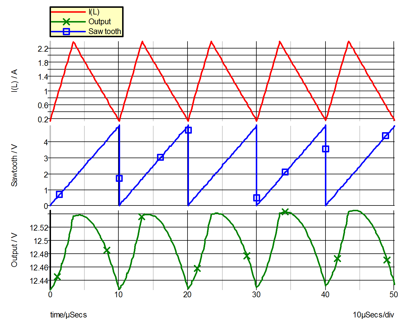 |
9.16 Waveforms for Example 5 |
| ◄ Example 4 -- Unregulated Converter | Example 6 -- Saturable Inductor ▶ |