Example 7 -- SCR with RL Load
The system studied in this example, as shown in fig. 9.20, is a sinusoidal voltage source rectified into an R-L load through a silicon controlled rectifier.
In this example, the SCR is modeled by the series combination of the simple switch S1 and the piecewise-linear resistor !R2, as shown in fig 9.21. The input file for this circuit is shown in fig 9.22. The comparator U2 (!D$U2 in the input file), the SR Flip Flop U1 (!D$U1 in the input file), and the elements E1, H1, and V5 together form a network that models the switching of the SCR. When a sufficient gate current is applied between the gate and the cathode, causing the voltage across the non-inverting input of U2 to exceed 2.5 V, the output of U2 will rise to approximately 5 V, thus setting the SR Flip Flop, which in turn causes the switch S1 to be closed. When S1 is closed, the model characteristic from anode to cathode is the series combination of a small resistance of the switch and a diode. On the other hand, if the SR flip flop is reset, the switch S1 will be opened, and the model characteristic from anode to cathode looks like a large resistor in series with a diode. The flip flop is reset when the voltage across its reset input, which is equal to the sum of the voltages across E1, H1, and V5, exceeds 2.500001 V. This situation occurs when the gate signal is absent and the current through the SCR is negative. The presence of E1 makes sure that the reset input does not reach its threshold value of 2.500001 V whenever there is a gate signal present. E1 accomplishes this by having its output equal to 500 V whenever the output of U2 reaches 5 V.
The variables of interest are the input voltage V(VI), the signal voltage V(VS), the current I(L1) through the inductor, and the voltage V(SCR) across the SCR. A differential voltage probe has been added to plot the latter. The waveforms associated with these variables as obtained from the simulation are shown in fig. 9.23.
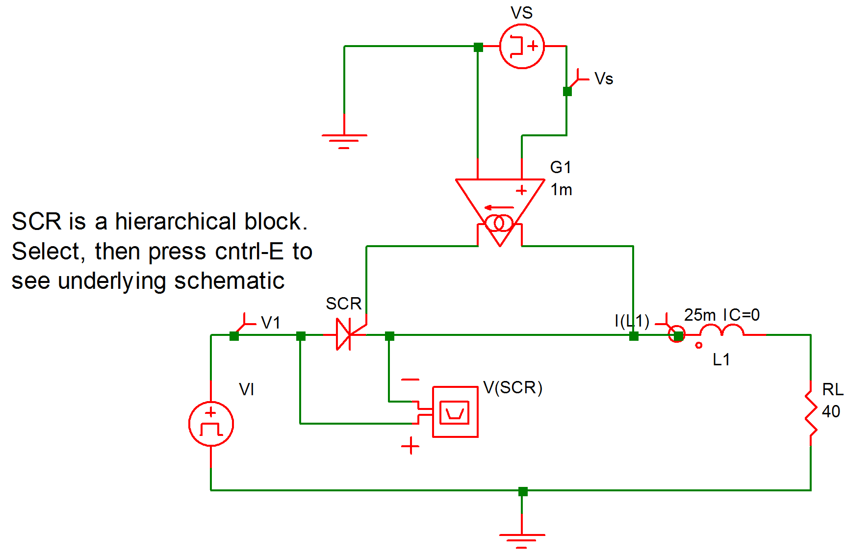 |
9.20 Example 7: A silicon-controlled rectifier with series R-L load. |
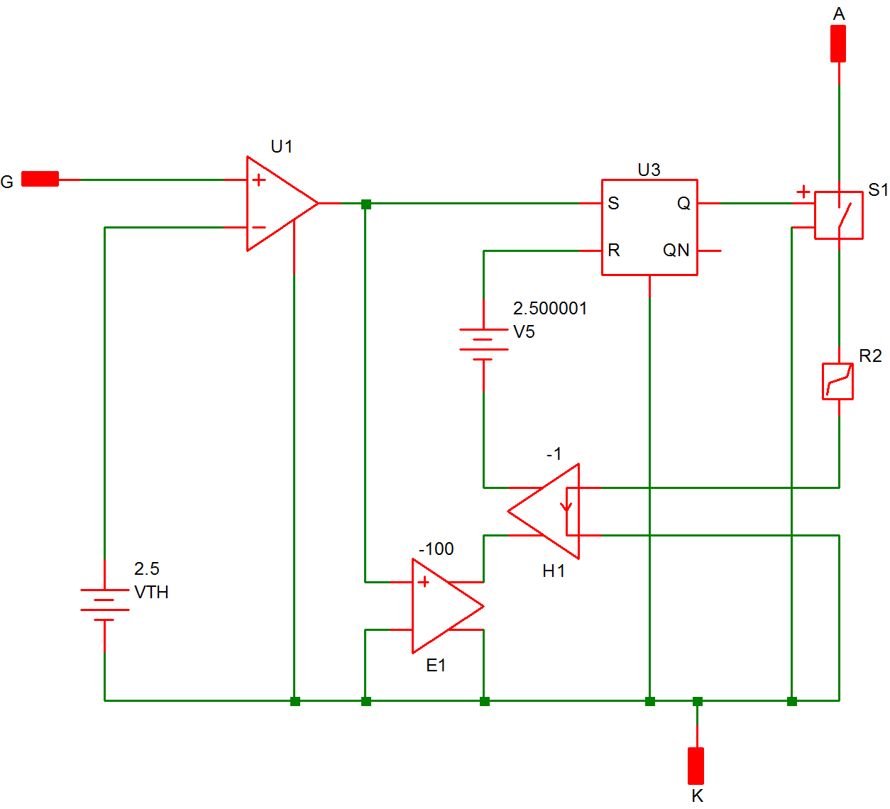 |
9.21 Piecewise-linear model of the SCR in terms of SIMPLIS elements |
* Sine Wave Driving A R-L Load Through A SCR

.PRINT  ALL
.OPTIONS  PSP_NPT=201
.TRAN 20m 0
VS 1 0 PUL V1=0 V2=1 FREQ=100 T_RISE=0 T_FALL=0 PWIDTH=400u
+ DELAY=1.1m OFF_UNTIL_DELAY=NO
X$SCR 4 2 3 scr1
L1 3 5 25m IC=0
E$Probe2$TP_DIFFPRB 6 0 4 3 1
RL 5 0 40
G1 3 2 1 0 1m
.SUBCKT scr1  12 11 10
.NODE_MAP A 12
.NODE_MAP G 11
.NODE_MAP K 10
X$U3 2 5 10 1 4 SIMPLIS_SRFF$1
V5 4 7 2.500001
X$U1 1 10 11 3 SIMPLIS_COMP$2
H1 7 9 VH1$TP_CCVS -1
VH1$TP_CCVS 8 10 0
E1 9 10 1 10 -100
VTH 3 10 2.5
!R$R2 6 8 R2$TP_SSPWLR IC=1
.MODEL R2$TP_SSPWLR VPWLR NSEG=2 X0=0 Y0=0 X1=1 Y1=1U
+ X2=1.1 Y2=2.000001
S1 12 6 2 10 S1$TP_SSVSW IC=Open
.MODEL S1$TP_SSVSW VCSW ROFF=10Meg RON=10u LOGIC=POS
+ TH=2.5 HYSTWD=20u
.SUBCKT SIMPLIS_COMP$2  201 100 101 102
!DCOMP 201 100 101 102 MCOMP IC=0
.MODEL MCOMP COMP RIN=5000 ROUT=50 VOL=0 VOH=5
+ HYSTWD=0.002 DELAY=0
.ENDS SIMPLIS_COMP$2
.SUBCKT SIMPLIS_SRFF$1  201 202 100 101 102
!D_SIMPLIS_SRFF 201 202 100 101 102 MSRFF IC=0
.MODEL MSRFF SRFF RIN=1e+007 ROUT=50 VOL=0 VOH=5
+ HYSTWD=2e-006 DELAY=0  TH=2.5 LOGIC=POS
.ENDS SIMPLIS_SRFF$1
.ENDS scr1
.END
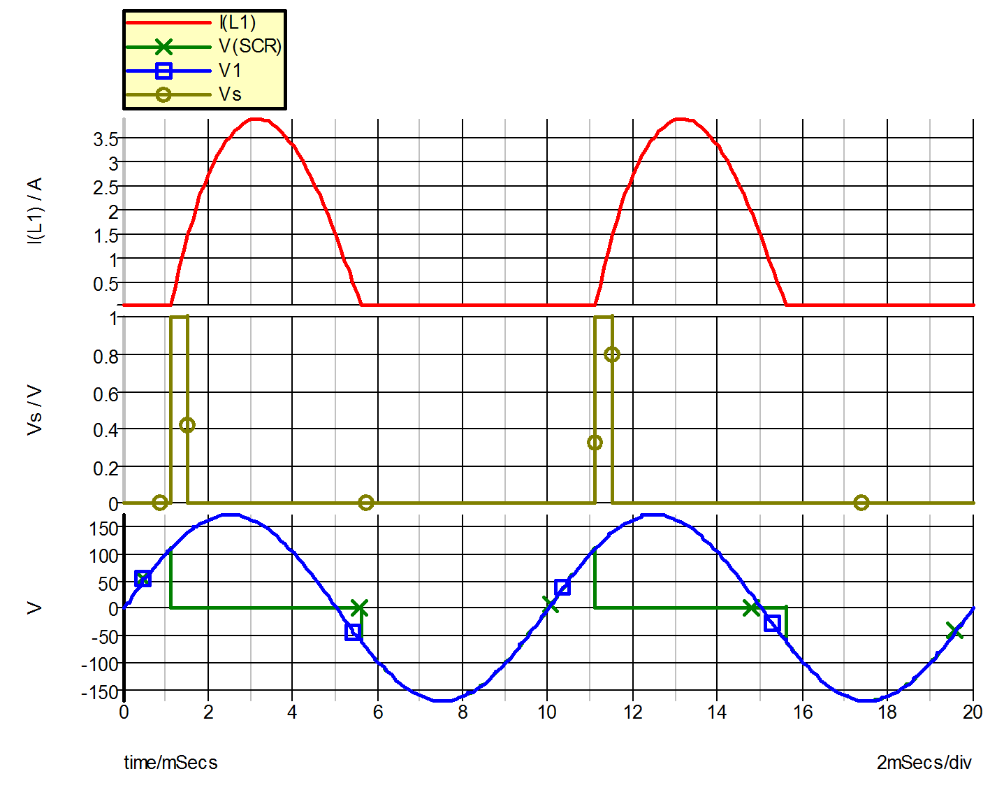 |
9.23 Waveforms for Example 7 |
| ◄ Example 6 -- Saturable Inductor | Overview ▶ |