Analog-Digital Interface Bridge
In this topic:
Netlist entry
Axxxx in out model_name
Connection details
| Name | Description | Flow | Type |
| in | Input | inout | g |
| out | Output | out | d |
Model format
.MODEL model_name adc_bridge parameters
Model parameters
| Name | Description | Type | Default | Limits |
| in_low | Maximum 0-valued analog input | real | 0.1 | none |
| in_high | Minimum 1-valued analog input | real | 0.9 | none |
| rise_delay | Rise delay | real | 1nS | ???MATH???1\text{e}^{-12} - \infty???MATH??? |
| fall_delay | Fall delay | real | 1nS | ???MATH???1\text{e}^{-12} - \infty???MATH??? |
| time_tol | Threshold time tolerance | real | 100pS | ???MATH???1\text{e}^{-12} - \infty???MATH??? |
| out_low | Used to calculate reflected static load. See text | real | 0 | none |
| out_high | Used to calculate reflected static load. See text | real | 5 | none |
| clamp_low | Clamp threshold 'ZERO' digital input. Default to out_low | real | out_low | none |
| clamp_high | Clamp threshold 'ONE' digital input. Default to out_high | real | out_high | none |
| clamp_res | Clamp minimum resistance | real | 1 | 1e-06 ???MATH???- \infty???MATH??? |
| clamp_bias | Clamp voltage | real | 0.8 | 0.2 - 2 |
| out_family | Output logic family | string | UNIV | none |
Device Operation
The analog-digital interface bridge is the main device used to connect analog signals to digital inputs. The device produces a digital signal that is in the logic '1' state when the analog input is above the high threshold (IN_HIGH) and a logic '0' state when it is below the low threshold (IN_LOW). When the analog input is in between these two states the output will be in the UNKNOWN state. The changes in state will be delayed according to the RISE_DELAY and FALL_DELAY parameters.
Analog input load
The analog input presents a load to its driving circuit according to the digital load that is being driven. In other words the digital load is reflected to the analog input. Both static (i.e. DC) and dynamic (i.e. capacitance) elements of the load are reflected. To accurately reflect the sink and source currents, the interface bridge needs to know the voltage levels of the device it is driving. The digital device will (usually) have a SINK_CURRENT and a SOURCE_CURRENT model parameter each of which apply at defined logic voltage levels. These levels must be specified in the OUT_LOW and OUT_HIGH parameters of the AD interface bridge model. The input is modelled by a current source in parallel with a resistor. The values of these components are calculated from the above mentioned parameters and the digital load.
Input clamp
The analog input is clamped at the voltages specified by CLAMP_LOW and CLAMP_HIGH. The clamping device has a characteristic similar but not identical to a junction diode in series with a resistance. Basically it has the characteristic of a diode up to a voltage excess of CLAMP_BIAS after which it becomes resistive with a dynamic resistance of CLAMP_RES. The diode characteristics are calculated so that the transition between the two regions is smooth.
Time Step Control - TIME_TOL parameter
Consider the following circuit and waveform
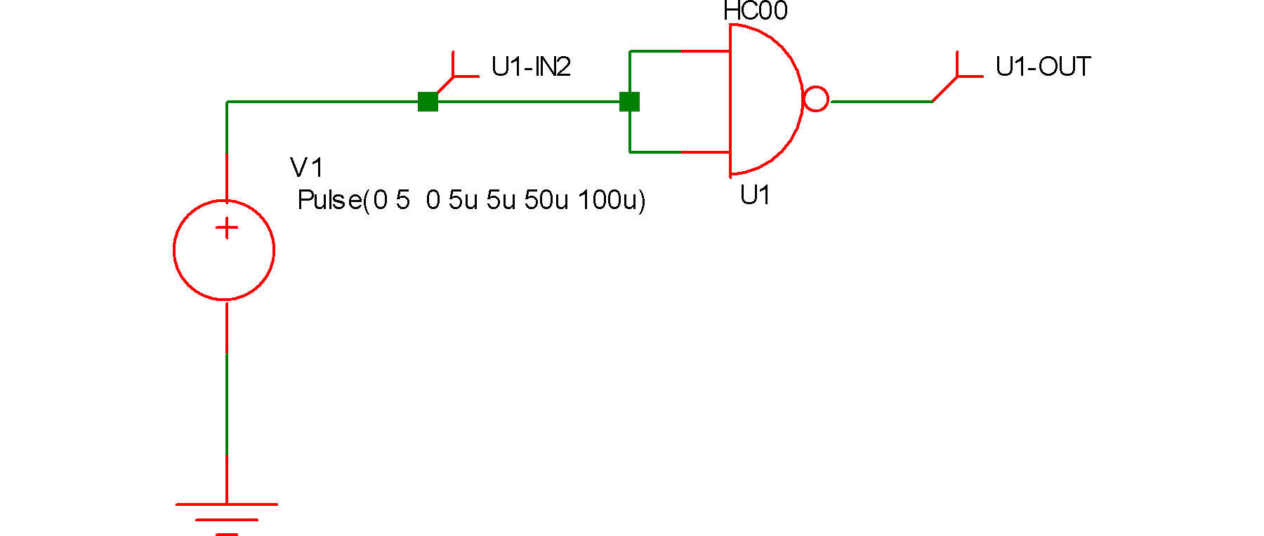
The graph shows the input and output of the NAND gate. Because the input is analog an implicit AD interface bridge will have been connected by the simulator. In the above example the parameters for this bridge have been set to:
.model HC_adc adc_bridge
+ in_low=2.1
+ in_high=2.2
+ rise_delay=1e-12
+ fall_delay=1e-12
+ out_family = "HC"
+ out_low = 0
+ out_high = 5
+ clamp_bias=0.5
+ clamp_res=10
+ time_tol=10u
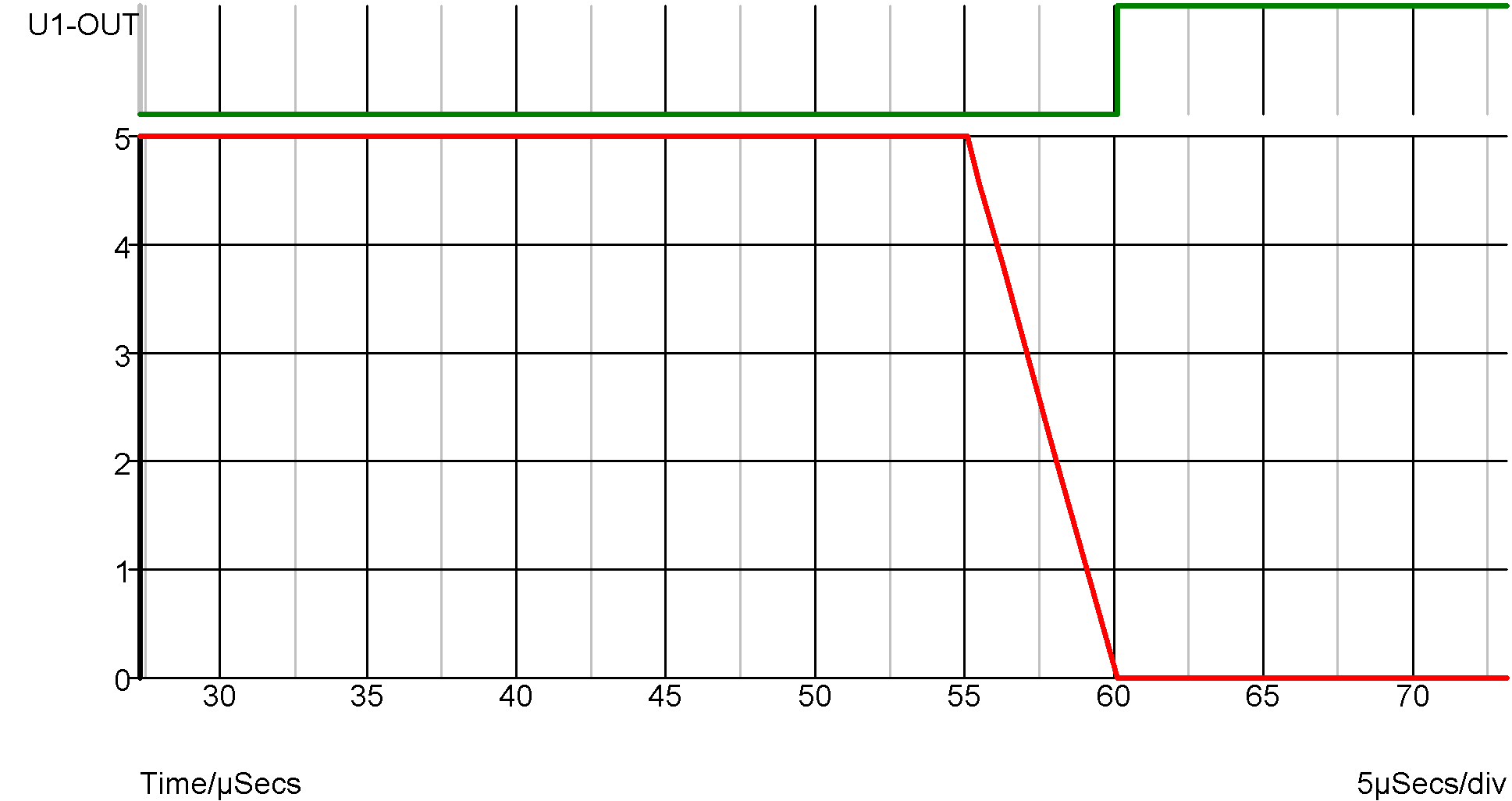
The last parameter, TIME_TOL has been deliberately set ridiculously high to demonstrate what happens without time step control on the input. The input thresholds of the HC gate are 2.1 and 2.2 volts yet the output in the above example doesn't switch until the input has reached 0V. Because there is little activity in the analog circuit, the time steps are quite large. In fact in the above example the transient timepoints are at 55uS, 55.04uS, 56.2uS, 57.8uS and 60uS. The timepoint at 57.8u is just before the 2.2 volt threshold is reached and it isn't until the next time point, 2.2uS later that the lower threshold is broken. The result is the location of the negative edge at the output is delayed by approx. 2.2uS from where it should be. The problem is that the analog system knows nothing of what is happening in the digital domain so carries on with large timesteps oblivious to the errors in the digital system.
To overcome this problem. SIMetrix features a mechanism (not in the original XSPICE system) that detects that the threshold has been passed and cuts back the time step to ensure that the digital edge occurs at an accurate point. The accuracy of this mechanism is controlled by the TIME_TOL parameter. The smaller this parameter, the more accurately the exact threshold will be hit at the expense of short time steps and longer simulation runs. TIME_TOL defaults to 100pS and in most applications this is a good choice. The following shows the result when TIME_TOL is set to the default.
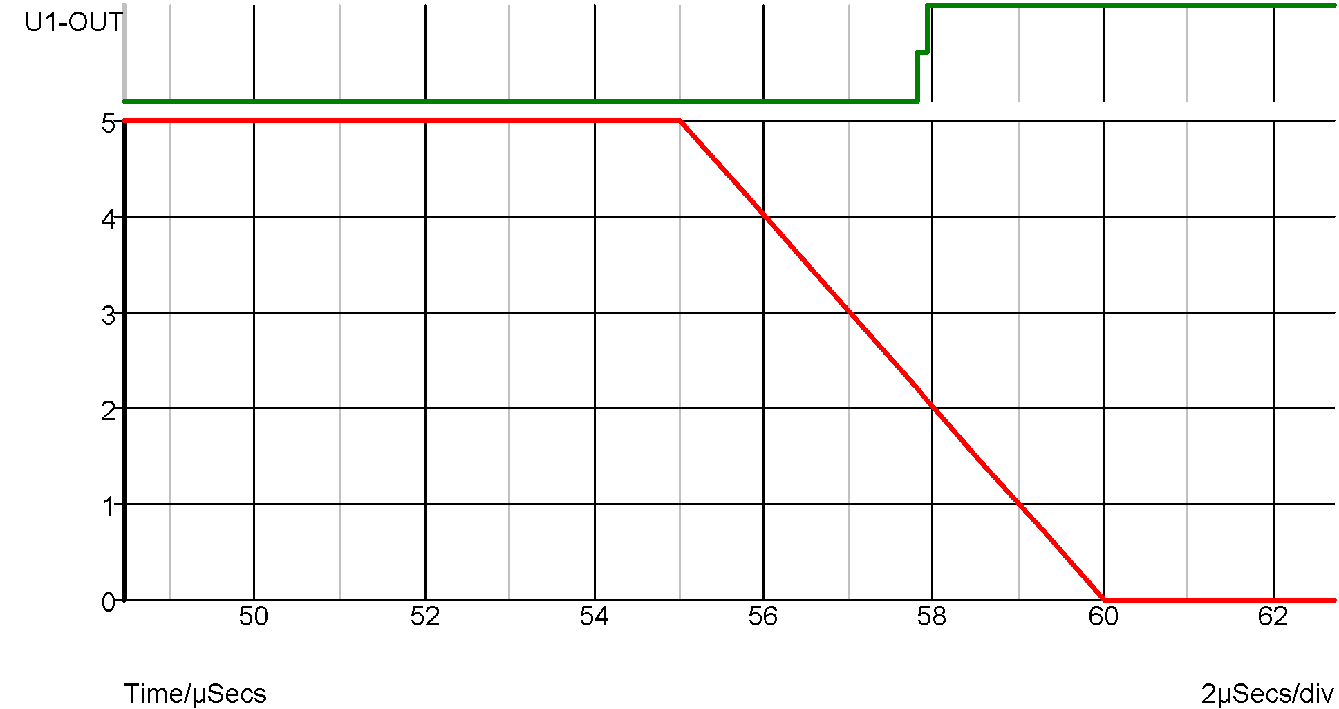
Here you can see the edge at the correct time.
The effect of not correctly simulating the threshold point has serious consequences when attempting to simulate relaxation oscillators constructed with digital inverters as the following graphs illustrate:
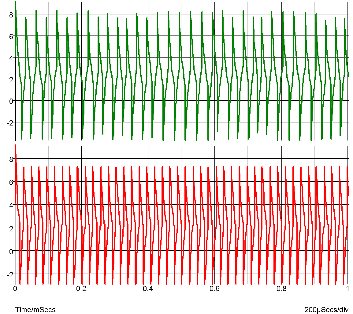
The top trace is without threshold control and the bottom trace is with it.
| ◄ Analog-Digital Converter | Digital-Analog Converter ▶ |