Asymmetric Delay
The Asymmetric Delay models a digital delay with different delay times for the rising and falling edges.
In this topic:
| Model Name: | Asymmetric Delay | |||
| Simulator: | This device is compatible with the SIMPLIS simulator. | |||
| Parts Selector Menu Location: | ||||
| Symbol Library: | None - the symbol is automatically generated when placed or edited. | |||
| Model Library: | None - the model is automatically generated when the simulation is run. | |||
| Subcircuit Names: |
|
|||
| Symbol: |
|
|||
| Multiple Selections: | Only one device at a time can be edited. | |||

Editing the Asymmetric Delay
To configure the Asymmetric Delay, follow these steps:
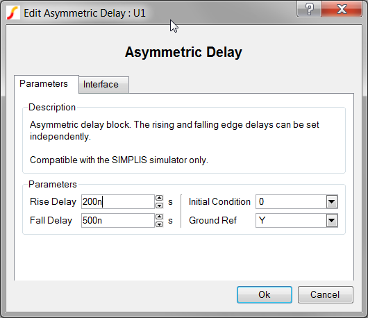
- Double click the symbol on the schematic to open the editing dialog to the Parameters tab.
- Make the appropriate changes to the fields described in the table below the image.
| Label | Parameter Description |
| Rise Delay | Delay from the rising edge of the input until the output changes |
| Fall Delay | Delay from the falling edge of the input until the output changes |
| Initial Condition | Initial condition of the Asymmetric Delay output at time=0 |
| Ground Ref | Determines whether or not a device has a ground reference pin. Any digital component that has an input or output pin connected to an analog circuit node must have its Ground Ref pin connected to an analog node. This is usually the ground on the schematic. |
To define the parameters for the interface between this digital component and each analog component connected directly to an input or output pin, follow these steps:
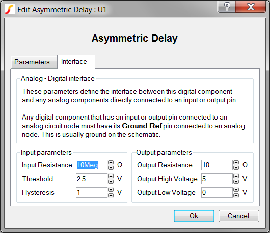
- From the Edit Asymmetric Delay dialog box, click on the Interface tab.
- Make the appropriate changes to the fields described in the table below the image.
| Label | Parameter Description | |||||||
| Input Resistance | Input resistance of each Asymmetric Delay input pin | |||||||
| Hysteresis, Threshold | 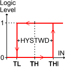 |
Hysteresis and
Threshold of the inputs. The hysteretic-window width, HYSTWD
is centered around Threshold (TH) voltage. To
determine the actual threshold ( TL , THI ),
substitute Threshold (TH) and Hysteresis
(HYSTWD) in each of the following formulas:
|
||||||
| Output Resistance | Output resistance of each Asymmetric Delay output pin | |||||||
| Output High Voltage | Output high voltage for each Asymmetric Delay output pin | |||||||
| Output Low Voltage | Output high voltage for each Asymmetric Delay output pin | |||||||
Examples
The test circuit used to generate the waveform examples in the next section can be downloaded here: simplis_022_asymmetricdelay_example.sxsch.
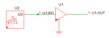
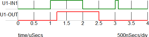
Waveforms
The waveforms below were taken from an Asymmetric Delay block with a rising edge delay of 200ns, and a falling edge delay of 500ns. The first input pulse is delayed as expected, while the second input pulse is not propagated to the output. This is because the second input pulse width is less than the propagation delay of the Asymmetric Delay.
Subcircuit Parameters
X$U1 2 1 SIMPLIS_DIGI1_D_ASYMMETRIC_DELAY_N vars: IC=0 RIN=10Meg ROUT=10 TH=2.5 HYSTWD=1.0
VOL=0 VOH=5 RISE_DELAY=2p FALL_DELAY=2p GNDREF='N'
| Parameter Name | Label | Data Type | Range | Units | Parameter Description | |||||||
| FALL_DELAY | Fall Delay | Number | 1f to 1024 | s | Delay from the falling edge of the input until the output changes | |||||||
| GNDREF | Ground Ref | String |
|
none | Determines whether or not a device has a ground reference pin. Any digital component that has an input or output pin connected to an analog circuit node must have its Ground Ref pin connected to an analog node. This is usually the ground on the schematic. | |||||||
| HYSTWD, TH |
Hysteresis, Threshold |
Number | min: 1f | V | |
Hysteresis and Threshold of the
inputs. The hysteretic-window width, HYSTWD is centered around
Threshold (TH) voltage. To determine the actual threshold (
TL , THI ), substitute Threshold (TH) and
Hysteresis (HYSTWD) in each of the following formulas:
|
||||||
| IC | Initial Condition | Number |
|
none | Initial condition of the Asymmetric Delay output at time=0 | |||||||
| RIN | Input Resistance | Number | min: 100 | Ω | Input resistance of each Asymmetric Delay input pin | |||||||
| RISE_DELAY | Rise Delay | Number | 1f to 1024 | s | Delay from the rising edge of the input until the output changes | |||||||
| ROUT | Output Resistance | Number | min: 1m | Ω | Output resistance of each Asymmetric Delay output pin | |||||||
| VOH | Output High Voltage | Number | any | V | Output high voltage for each Asymmetric Delay output pin | |||||||
| VOL | Output Low Voltage | Number | any | V | Output high voltage for each Asymmetric Delay output pin | |||||||