Parameterized Linear Regulator
The Parameterized Linear Regulator models a linear regulator with an adjustable maximum output and short circuit current.The model is implemented as a two segment piecewise linear device where the first segment ramps the output voltage to follow the input voltage and the second segment has a slope near 0 to model the output voltage in regulation.
In this topic:
| Model Name: | Linear Regulator With Line & Load Regulation and turn-on/-off | |
| Simulator: |
|
This device is compatible with the SIMPLIS simulator |
| Parts Selector Menu Location: | ||
| Symbol Library: | simplis_analog_functions.sxslb | |
| Model File: | simplis_analog_functions.lb | |
| Symbol Name: | SIMPLIS_LINEAR_REG | |
| Subcircuit Name: | SIMPLIS_LINEAR_REG_BB | |
| Symbol: | 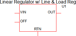
|
|
| Multiple Selections: | Multiple devices can be selected and edited simultaneously. | |
Previous Version Compatibility
This model and symbol was introduced with version 8.2; however, the model and supporting files are identical to the Parameterized Voltage Reference.
For a version of the Parameterized Voltage Reference editable with versions prior to version 7.20, see the parts selector entry:
Editing the Parameterized Linear Regulator
To configure the Linear Regulator, follow these steps:
- Double click the symbol on the schematic to open the editing dialog.
- Change the I/O Characteristics and Parameters.
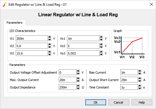
| Parameter Label | Units | Description |
| Vi1 | V | First input voltage point that defines the response characteristic. |
| Vi2 | V | Second input voltage point that defines the response characteristic. |
| Vi3 | V | Third input voltage point that defines the response characteristic. |
| Vr1 | V | First output voltage point that defines the response characteristic. |
| Vr2 | V | Second output voltage point that defines the response characteristic. |
| Vr3 | V | Third output voltage point that defines the response characteristic. |
| Output Voltage Offset Adjustment | V | DC offset for the regulated output voltage. |
| Max. Output Current | A | Maximum output current. If the output current exceeds this value, the output voltage will start to decrease. |
| Output Impedance | Ω | Output impedance of the reference. |
| Bias Current | A | Input bias current. |
| Output Short Current | A | Current supplied by the reference during an output short circuit event. |
| Time Constant | s | Internal time constant. |
Examples
Below are two examples which demonstrate certain aspects of the linear regulator.
Example 1 - Startup Behavior
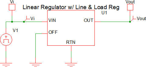
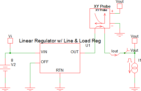
The test circuit used to generate the waveform examples in the next section can be downloaded here: simplis_083_linear_reg_ramp_input.sxsch.
Example 1 - Waveforms
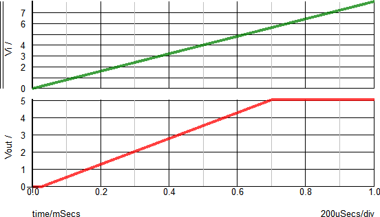
The waveforms shown below are for a test circuit with a ramped input voltage. A brief description of the behavior is as follows, with the dialog below used for reference:
- At t=0μs, the input voltage (Vi) starts at 0V and begins to ramp up to a final voltage of 8V.
- At t=25μs, the input voltage will reach 200mV (Vi1 above). This will correlate to an output voltage of 1mV (Vr1 above).
- At t=700μs, the input voltage will reach 5.6V (Vi2 above). This will correlate to an output voltage of 5V (Vr2 above). At this point, the regulator is at the regulation point.
- At t>700μs, the output voltage will remain ~5V and will rise linearly based on Vi3 and Vr3. In a typical application, the input voltage range from Vi2 to Vi3 is when the output is in regulation.
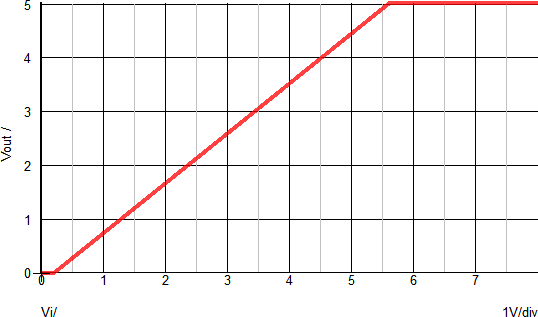
The X-Y plot below helps to visualize the relationship between the input voltage (Vi) and the output voltage (Vr). The X-Axis shows the input voltage and the Y-Axis show the regulated output voltage. With no load applied, the inflection points should closely match the Vi and Vo points defined in the dialog.
Example 2 - Ramped Load
The test circuit used to generate the waveform examples in the next section can be downloaded here: simplis_083_linear_reg_ramp_load.sxsch.
Example 2 - Waveforms
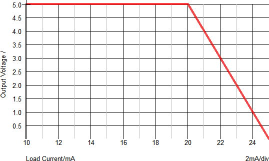
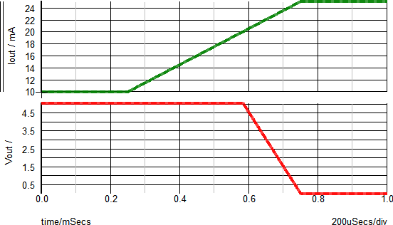
The waveforms shown below are for a test circuit with a ramped load current. A brief description of the behavior is as follows, with the dialog below used for reference:
- At t=0μs, the load current starts at 10mA.
- At t=250μs, the load current starts to ramp and continues to a final value of 25mA.
- At t=~580μs, the load current reaches the Max. Output Current value of 20mA.
- At t>580μs, the regulated output voltage will begin to decrease as the load current increases.
- At t=750μs, the load current will reach the Output Short Circuit current value of 25mA. At this point, the output voltage will be ~0V.
The X-Y plot below helps to visualize the relationship between the regulated output voltage and the output current. The X-Axis shows the output voltage and the Y-Axis show the load current. You can see that as the load current increases above the Max. Output Current value (20mA), the output voltage will decrease.