5.1 Building a Compensator
In this section of the tutorial, you will build a standard 3-pole, 2-zero voltage-mode compensator using a built-in parameterized OpAmp and passive components.
After finishing this section, you will have a
complete closed-loop synchronous buck switching power supply model like the following: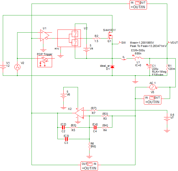
In this topic:
Key Concepts
This topic addresses the following key concepts:
- Symbols can use variables, or parameterized values, that help with schematic reuse. For maximum flexibility, the compensator schematic uses parameterized values.
- Each schematic has a command (F11) window which stores analysis directives and variable statements. The text in the F11 window is included in the simulation deck.
- Parameter values can be assigned or calculated in the command (F11) window.
What You Will Learn
- How to parameterize symbols using expressions and the F11 window.
- Why, based on how POP works, choosing the switching node as the periodic input in section 3.2 Set up a POP Analysis was not the ideal choice.
- How to solve a common POP simulation error by selecting a different POP trigger schematic node.
- How to add parameter debug statements to the F11 window.
5.1.1 Build the Compensator Schematic
| Symbol | Parts Selector Location | Keyboard Shortcut |
| Multi-Level Parameterized Opamp (Version 8.0+) | Analog Functions | none |
| Resistor | Commonly Used Parts | 4 |
| Capacitor (Ideal) | Commonly Used Parts | C |
| Power Supply | Commonly Used Parts | V |
| Bode Plot Probe (Gain/Phase) w/ Measurements | Commonly Used Parts | none |
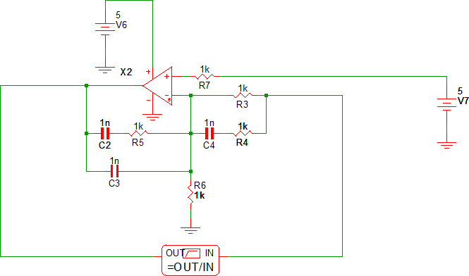
5.1.2 Assign Parameterized Values to Symbols
After you have the drawn your schematic, double check that each resistor and capacitor has the reference designator as shown in the schematic above.
- Select the resistor or capacitor symbol.
- Press Shift+F8.Result: A dialog opens for you to enter a new reference designator.
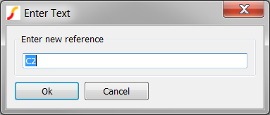
- Enter the reference designator as shown in the schematic above.
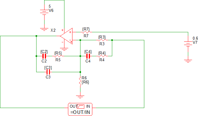
When you assign parameterized values, you enclose the parameter name or expression in curly braces. In this tutorial you will use the reference designator text as the parameter name, for example, the parameterized value for the resistor R3 will be {R3}.
- Double click on each resistor or capacitor and change the value of the resistance or capacitance to a parameterized value.
- For the DC source V7, change the value to 0.6V. Tip: This will be the reference voltage for the compensator.
Your compensator schematic should now look like the following:
5.1.3 Connect the Compensator to the Power Stage
You will now close the feedback loop by connecting the compensator to the power stage.
- Delete V3, the DC source which was the duty cycle control.
- Delete the wires connecting the AC source V5 to the comparator U1 input.
- Move V5 to the right side of the schematic.Tip: This will become the loop perturbation source.
- Wire the compensator to the power stage as shown in the image below:
- Add the Bode Plot Probe across the V5 source. Tip: This will probe the loop gain of the converter.
- The output capacitor in this design has no ESR. In the previous simulations this was
not an issue, but when the compensator is added, the ESR plays a role in calculating the
compensator values. To include an ESR on this multi-level capacitor, double-click on
C1 and set the model level to 2, and assign an ESR of 4mΩ.Result: The ESR value of 4m is displayed on the schematic. This indicates the model for the capacitor now includes an ESR.
5.3.4 Disable Power Stage and Compensator Bode Plot Probes
You now have three Bode Plot probes on the schematic and each probe will output a gain and phase curve with the default names of Gain and Phase. This will make a confusing graph with six curves, so in the next procedure, you will turn off the compensator and power stage probes as well as rename the curves generated by these probes. This will allow easy debugging later when you might want to see the power stage or compensator bode plots.
- Double click on the compensator bode plot probe and rename the gain and phase curves to Compensator Gain and Compensator Phase.
- Check Disable gain/phase at the top of the dialog, and then click Ok.
- Double click on the power stage bode plot probe and rename the gain and phase curves to Plant Gain and Plant Phase.
- Check Disable gain/phase at the top of the dialog, and then click Ok.
5.1.5 Enter Parameter Values in the Command (F11) Window
In 5.1.3 Connect the Compensator to the Power Stage, you added parameterized values to each symbol by enclosing the variable name in curly braces { }. The curly braces form an expression and tell the program to stop and evaluate the expression; in this case, the program simply substitutes the value for the variables R3, C2, etc. in place of the expressions, {R3}, {C2}, etc. At this point in the design, the values for the compensator are not defined. Next, you will assign values to these variables using .VAR statements.
Explaining how to compensate a 3-Pole/2-Zero voltage mode compensator is beyond the scope of this tutorial. Instead of dwelling on the compensator design process, which was taken from this application note, you will copy the text lines from this tutorial and paste them into the F11 window of the schematic. The .VAR lines are actually an entire design process taken from a spreadsheet and turned into variable statements.
To enter the parameter values in the F11 window, follow these steps.
- Copy all text in the box below:
****************************** *** Circuit Specifications *** ****************************** .VAR VIN = 12 .VAR VRAMP = 1 .VAR L = 680n .VAR C = 220u .VAR VOUT = 1.2 .VAR VREF = 0.6 .VAR ESR = 4m .VAR FXOVER = 80k .VAR FSW = 500k *** Calculated Parameters - not used in calculations .VAR FLC = 13012.31 .VAR FESR = 180857.89 .SUBCKT ONE_PULSE_SOURCE_I 1 2 vars: _T_RISE=0 _T_FALL=0 _DELAY=0 _V1=0 _V2=1 _PWIDTH=1u .NODE_MAP P 1 .NODE_MAP N 2 {'*'} _DELAY : {_DELAY} {'*'} _T_RISE : {_T_RISE} {'*'} _PWIDTH : {_PWIDTH} I1 1 2 PWL NSEG=4 X0=0 Y0={_V1} X1={_DELAY} Y1={_V1} X2={_DELAY+_T_RISE} Y2={_V2} X3={_DELAY+_T_RISE+_PWIDTH} Y3={_V2} X4={_DELAY+_T_RISE+_PWIDTH+_T_FALL} Y4={_V1} .ENDS ********************************************************* *** Compensator Design - Find desired poles and zeros *** ********************************************************* *** Place Second Zero at LC .VAR FZ2 = {1/(2*pi*SQRT(L*C))} *** Place First Zero at 75% of FZ2 .VAR FZ1 = {0.75*FZ2} *** Place Second Pole (1st pole at origin) at ESR zero .VAR FP2 = {1/(2*pi*ESR*C)} *** You will get better performance putting the pole *** above ESR zero (different than design procedure) .VAR FP2 = {0.75*FSW} *** Place Third Pole at 1/2 the switching frequency .VAR FP3 = {0.5*FSW} ******************************************************************* *** Compensator Design - Assign resistor and capacitor values *** *** The design procedure was taken from IR/Infineon an-1162.pdf *** *** *** *** http://www.irf.com/technical-info/appnotes/an-1162.pdf *** ******************************************************************* *** Choose C4 to be 2.2nF This is somewhat arbitrary, *** it sets the magnitude of other compensator values. .VAR C4 = 2.2n *** From C4 and FP2, Calculate R4 .VAR R4 = {1/(2*pi*C4*FP2)} *** From C4, R4 and FZ2, Calculate R3 .VAR R3 = {1/(2*pi*C4*FZ2)-R4} *** From R3, VREF and Nominal VOUT, Calculate R6 .VAR R6 = {R3*VREF/(VOUT-VREF)} *** Calculate R7 as the parallel combination of R3 and R6 .VAR R7 = {R3*R6/(R3+R6)} *** Calculate R5. Modify VRAMP to adjust final loop characteristics .VAR R5 = {2*pi*FXOVER*L*C*VRAMP/(VIN*C4)} *** From R5 and FZ1, Calculate C2 .VAR C2 = {1/(2*pi*R5*FZ1)} *** From R5 and FP3, Calculate C3 .VAR C3 = {1/(2*pi*R5*FP3)} ***************************************************************** *** Debug. These statements come out in the deck as comments. *** *** Simulator -> Edit Netlist (after preprocess) opens file *** ***************************************************************** {'*'} FZ2 : {FZ2} {'*'} FZ1 : {FZ1} {'*'} FP2 : {FP2} {'*'} FP3 : {FP3} {'*'} C4 : {C4} {'*'} R4 : {R4} {'*'} R3 : {R3} {'*'} R6 : {R6} {'*'} R5 : {R5} {'*'} C2 : {C2} {'*'} C3 : {C3} - In the schematic editor, press F11.Result: The command (F11) window opens at the bottom of the schematic.
- Drag the splitter bar between the command (F11) window and the schematic so the command window and the schematic take approximately 50% of the vertical space.
- In the command window, scroll down past the last statement, which is the
.SIMULATOR DEFAULT
line and use the keyboard shortcut Ctrl+V to paste the copied text in the F11 window below the .SIMULATOR DEFAULT line.
Four sections of text are used to parameterize the compensator.
- The first section has design values. The statement .VAR VIN = 12 assigns the number 12 to the variable VIN. Although VIN is not used in the schematic, it is used in calculations for other variables. You could add VIN to the input source as a parameter {VIN}.
- The second section has the calculations for the compensator poles and zeros. The
statement .VAR FZ2 = {1/(2*pi*SQRT(L*C))} assigns a value to the
FZ2 variable. In this case, the value is the resonant frequency of the converter.
Note: The variables L and C, as well as the global constant pi and the built-in function SRQT(), are used in the expression on the right side of the equals sign. The variables L and C must be assigned before they are used; therefore, the order of the lines in the window is important. The global constant pi and the function SQRT() are defined by the program.
- The third section calculates the actual resistor and capacitor values from the first section of the circuit specifications and the poles and zeros from the second section.
- The final section has debug statements. These statements output comments to the
simulation deck so you can easily debug which values are being used in the compensator.
For example, the values in the design will output the following to the deck file:
* FZ2 : 13012.3080131893
* FZ1 : 9759.23100989196
* FP2 : 375000
* FP3 : 250000
* C4 : 2.2e-009
* R4 : 192.915082535631
* R3 : 5366.67940889006
* R6 : 5366.67940889006
* R5 : 2848.37733925475
* C2 : 5.72541552580328e-009
* C3 : 2.23502610975745e-010
A schematic saved at this state can be downloaded here: 10_SIMPLIS_tutorial_buck_converter.sxsch.
5.1.6 Try to Simulate the Design
When you try to simulate this design you will get simulation errors and SIMPLIS will automatically run a transient simulation so you can see what might be causing the errors. The waveforms will appear as follows:
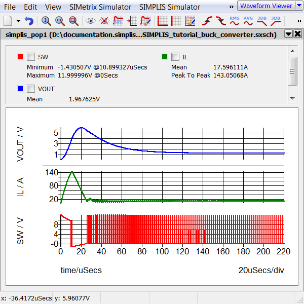
Clearly, the converter reaches a steady state operating point at the end of the transient simulation so you know that the loop is stable. The cause for the simulation errors is as follows:
- The initial conditions for the converter cause the error: the output voltage starts at 0V, and the compensator attempts to correct this with several cycles of full duty cycle.
- The modulator, at this stage of development, does not have either a duty cycle limit or a current limit; as a result, the inductor current reaches a high value before the output voltage overshoots.
- After the output voltage overshoots the reference, the compensator turns off the switch for several switching periods.
- During the portion of the simulation where there is no switching, SIMPLIS is monitoring the POP Trigger and at 4.4μs, when twice the maximum POP period is reached, SIMPLIS thinks something has gone wrong with the circuit and outputs the following warning and error:
*** WARNINGS REPORTED BY SIMPLIS ***
****************************************
<<<<<<<< Error Message ID: 5020 >>>>>>>>

Periodic Operating-Pt Analysis:

    Reaching a time duration equal to
    `4.40000e-006' without registering the
    triggering condition that defines
    the start of a period.  Check your
    circuit and/or initial conditions.

*** END SIMPLIS WARNING REPORT ***

*** ERRORS REPORTED BY SIMPLIS ***
****************************************
<<<<<<<< Error Message ID: 5039 >>>>>>>>

The periodic operating point (POP) analysis
has failed to converge.  AC analysis will
not be performed.


*** END SIMPLIS ERROR REPORT ***
- Solution 1: Change the initial conditions of the circuit to initialize the circuit closer to the steady-state conditions. The compensator will then make small corrections to bring the converter into steady-state; the duty cycle will never reach 0 or 100%; and the POP analysis will succeed. This is a good design practice and you will probably need to do this at some point, especially with a more complex circuit.
- Solution 2: Change the location of the POP trigger gate so that the input signal crosses the POP trigger threshold on every switching cycle, independent of the commanded duty cycle. Since the oscillator node is independent of the commanded duty cycle, this is a good choice for the POP trigger node.
5.1.7 Move the POP Trigger Gate
- Click on the POP trigger symbol to select it.
- Press Ctrl+X to cut the symbol.
- Press Ctrl+V to paste the symbol.
- Place the POP trigger symbol to the right of the oscillator V2.
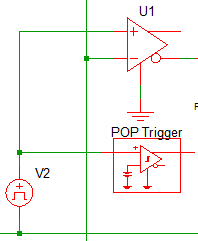
- Double click on the POP trigger symbol, and change the Threshold parameter to 0.5V and click Ok to save your changes.
- Wire the input of the POP Trigger to V2 as shown in the image.
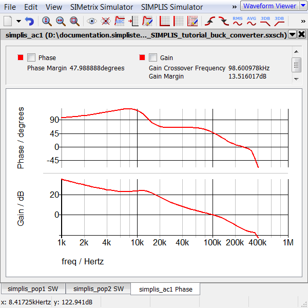
5.1.8 Verify Loop Stability
The circuit should now run the POP and AC analysis configured earlier in the tutorial; however, the maximum frequency for the AC sweep is greater than the switching frequency which will result in plots with a small scale due to the high frequency noise.
To change the maximum frequency, follow these steps:
- From the schematic editor menu, select .
- In the Sweep parameters section on the AC tab, change the Stop frequency to 400kHz.
- Click Ok, or press F9 to run the simulation.Result: The simulation runs without errors and the bode plot for the converter is output to the waveform viewer. The Gain Crossover Frequency is 98kHz, the Phase Margin is 48 degrees and the Gain Margin is 13.5dB.
5.1.9 Save your Schematic
To save your schematic, follow these steps:
- From the menu bar, select .
- Navigate to your working directory where you are saving your schematics.
- Name the file 11_my_buck_converter.sxsch.
A schematic saved at this state can be downloaded here: 11_SIMPLIS_tutorial_buck_converter.sxsch.