Parameterized Voltage Reference
The Parameterized Voltage Reference models a voltage reference with an adjustable maximum output voltage and short circuit current. The model is implemented as a two segment piecewise linear device where the first segment ramps the reference voltage to follow the input voltage and the second segment has a slope near 0 to model the reference voltage in regulation.
In this topic:
| Model Name: | Voltage Reference With Line & Load Regulation and turn-on/-off | |
| Simulator: |
|
This device is compatible with the SIMPLIS simulator |
| Parts Selector Menu Location: | ||
| Symbol Library: | simplis_analog_functions.sxslb | |
| Model File: | simplis_analog_functions.lb | |
| Symbol Name: | SIMPLIS_VREF_LINE_LOAD_REG | |
| Subcircuit Name: | SIMPLIS_VREF_LINE_LOAD_REG_BB | |
| Symbol: | 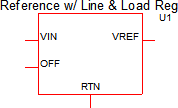
|
|
| Multiple Selections: | Multiple devices can be selected and edited simultaneously. | |
Previous Version Compatibility
This symbol was introduced with version 8.0; however, the model and supporting files are available in version 7.20 as well. In versions prior to 7.20, the schematic will simulate, but you will not be able to edit the parameters with the dialog pictured in this topic.
For a version of the Parameterized Voltage Reference editable with versions prior to version 7.20, see the parts selector entry:
Symbol Migration
Symbols placed on schematics in previous versions of SIMetrix/SIMPLIS can be automatically migrated to use the new symbols. The schematic tools menu will invoke a routine which migrates the existing symbols to the new symbols. As this action makes substantial changes to the schematic, it is recommended that you save a backup copy of the schematic first.
Editing the Parameterized Voltage Reference
To configure the Voltage Reference, follow these steps:
- Double click the symbol on the schematic to open the editing dialog.
- Change the Reference I/O Characteristics and Parameters.
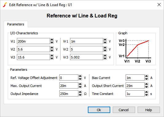
| Parameter Label | Units | Description |
| Vi1 | V | First input voltage point that defines the response characteristic. |
| Vi2 | V | Second input voltage point that defines the response characteristic. |
| Vi3 | V | Third input voltage point that defines the response characteristic. |
| Vr1 | V | First output voltage point that defines the response characteristic. |
| Vr2 | V | Second output voltage point that defines the response characteristic. |
| Vr3 | V | Third output voltage point that defines the response characteristic. |
| Ref. Voltage Offset Adjustment | V | DC offset for the output reference voltage. |
| Max. Output Current | A | Maximum output current. If the output current exceeds this value, the output voltage will start to decrease. |
| Output Impedance | Ω | Output impedance of the reference. |
| Bias Current | A | Input bias current. |
| Output Short Current | A | Current supplied by the reference during an output short circuit event. |
| Time Constant | s | Internal time constant. |
Examples
Below are two examples which demonstrate certain aspects of the voltage reference.
Example 1 - Startup Behavior
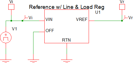
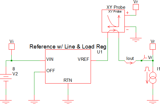
The test circuit used to generate the waveform examples in the next section can be downloaded here: simplis_082_voltage_reference_ramp_input.sxsch.
Example 1 - Waveforms
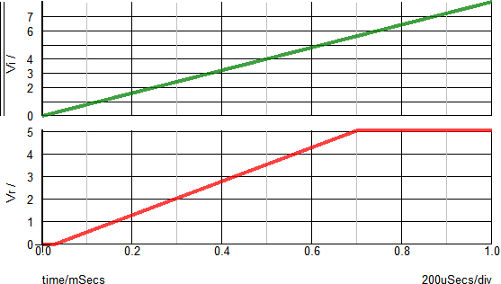
The waveforms shown below are for a test circuit with a ramped input voltage. A brief description of the behavior is as follows, with the dialog below used for reference:
- At t=0μs, the input voltage (Vi) starts at 0V and begins to ramp up to a final voltage of 8V.
- At t=25μs, the input voltage will reach 200mV (Vi1 above). This will correlate to an output voltage of 1mV (Vr1 above).
- At t=700μs, the input voltage will reach 5.6V (Vi2 above). This will correlate to an reference voltage of 5V (Vr2 above). At this point, the reference is at the regulation point.
- At t>700μs, the output voltage will remain ~5V and will rise linearly based on Vi3 and Vr3. In a typical application, the input voltage range from Vi2 to Vi3 is when the reference is in regulation.
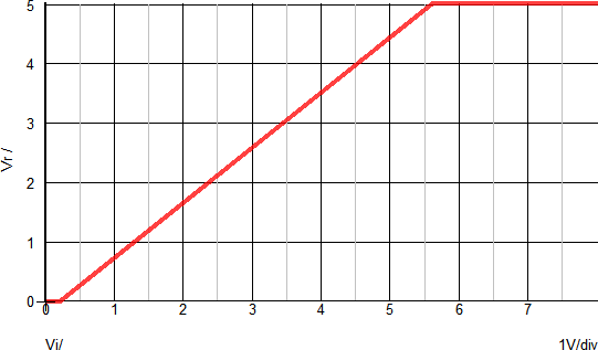
The X-Y plot below helps to visualize the relationship between the input voltage (Vi) and the output voltage (Vr). The X-Axis shows the input voltage and the Y-Axis show the reference voltage. With no load applied, the inflection points should closely match the Vi and Vr points defined in the dialog.
Example 2 - Ramped Load
The test circuit used to generate the waveform examples in the next section can be downloaded here: simplis_082_voltage_reference_ramp_load.sxsch.
Example 2 - Waveforms
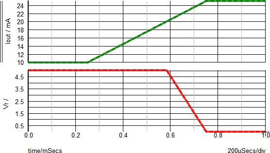
The waveforms shown below are for a test circuit with a ramped load current. A brief description of the behavior is as follows, with the dialog below used for reference:
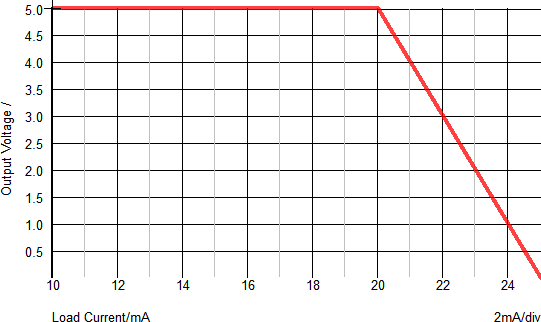
- At t=0μs, the load current starts at 10mA.
- At t=250μs, the load current starts to ramp and continues to a final value of 25mA.
- At t=~580μs, the load current reaches the Max. Output Current value of 20mA.
- At t>580μs, the reference output voltage will begin to decrease as the load current increases.
- At t=750μs, the load current will reach the Output Short Circuit current value of 25mA. At this point, the reference output voltage will be ~0V.
The X-Y plot below helps to visualize the relationship between the reference voltage and the output current. The X-Axis shows the output voltage and the Y-Axis show the load current. You can see that as the load current increases above the Max. Output Current value (20mA), the reference voltage will decrease.