Digital Pulse Source
The Digital Pulse Source provides a single bit periodic digital signal. This device is most often used to generate digital clocks.
For generating multi-bit signals see the Digital Signal Source.
In this topic:
| Model Name: | Digital Pulse Source | |||||||||
| Simulator: | This device is compatible with the SIMPLIS simulator. | |||||||||
| Parts Selector Menu Location: | ||||||||||
| Symbol Library: | None - the symbol is automatically generated when placed or edited. | |||||||||
| Model Library: | SIMPLIS_DIGI1.LB | |||||||||
| Subcircuit Names: |
|
|||||||||
| Symbols: |
|
|||||||||
| Multiple Selections: | Only one device at a time can be edited. | |||||||||


Editing the Digital Pulse Source
To configure the Digital Pulse Source, follow these steps:
- Double click the symbol on the schematic to open the editing dialog to the Parameters tab.
- Make the appropriate changes to the fields described in the table below the image.
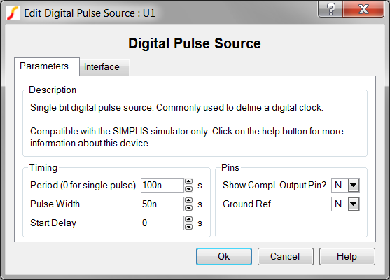
| Label | Parameter Description |
| Period (0 for single pulse) | Pulse generator oscillation period. |
| Pulse Width | Time interval between the rising edge and falling edge of a the non-inverted output. |
| Start Delay | Delay time at which the non-inverting output transitions from a logic low to a logic high and the complementary output pin transitions from a logic high to a logic low. |
| Show Compl. Output Pin? | Determines whether or not a device has a complementary output. |
| Ground Ref | Determines whether or not a device has a ground reference pin. Any digital component that has an input or output pin connected to an analog circuit node must have its Ground Ref pin connected to an analog node. This is usually the ground on the schematic. |
To define the parameters for the interface between this digital component and each analog component connected directly to an input or output pin, follow these steps:
- From the Edit Digital Pulse Source dialog box, click on the Interface tab.
- Make the appropriate changes to the fields described in the table below the image.
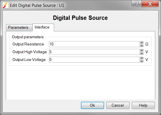
| Label | Parameter Description |
| Output Resistance | Output resistance of each output pin. |
| Output High Voltage | Output high voltage of each output pin. |
| Output Low Voltage | Output low voltage of each output pin. |
Examples
The test circuit used to generate the waveform examples in the next section can be downloaded here: simplis_021_digitalpulsesource_example.sxsch.
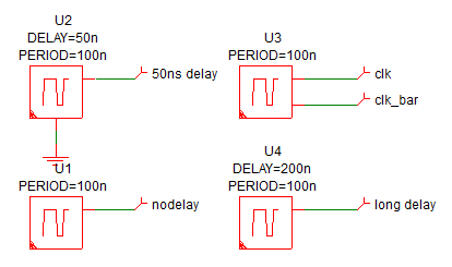
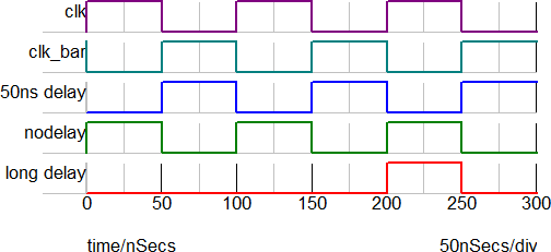
Waveforms
The waveforms below were taken from the state machine example described in the SIMPLIS Lookup Table with Don't Care Input Definitions.
Subcircuit Parameters
X$U1 5 SIMPLIS_DIGI1_D_PULSE_N_N vars: PERIOD=100n WIDTH=50n DELAY=0 ROUT=10 VOL=0 VOH=5 COMP='N' GNDREF='N'
| Parameter Name | Label | Data Type | Range | Units | Parameter Description |
| COMP | Show Compl. Output Pin? | String |
|
none | Determines whether or not a device has a complementary output. |
| DELAY | Start Delay | Number | 0 to 1024 | s | Delay time at which the non-inverting output transitions from a logic low to a logic high and the complementary output pin transitions from a logic high to a logic low. |
| GNDREF | Ground Ref | String |
|
none | Determines whether or not a device has a ground reference pin. Any digital component that has an input or output pin connected to an analog circuit node must have its Ground Ref pin connected to an analog node. This is usually the ground on the schematic. |
| PERIOD | Period (0 for single pulse) | Number | min: 0 | s | Pulse generator oscillation period. |
| ROUT | Output Resistance | Number | min: 1m | Ω | Output resistance of each output pin. |
| VOH | Output High Voltage | Number | any | V | Output high voltage of each output pin. |
| VOL | Output Low Voltage | Number | any | V | Output low voltage of each output pin. |
| WIDTH | Pulse Width | Number | min: 0 | s | Time interval between the rising edge and falling edge of a the non-inverted output. |