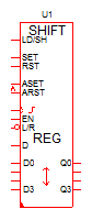
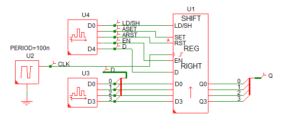
Shift Register (Right)
The Shift Register (Right) models a combination of a clocked data type register and a shift register with right shifts only. The clock edge for the register can be set with the Trigger Condition parameter to be a rising edge (0_TO_1) or a falling edge (1_TO_0). The set/reset events can be configured to be asynchronous or synchronous to the clock with the Set/Reset Type parameter. The active logic level of the inputs can be configured with the Set/Reset Level and Load/Shift Level parameters.
For the right shift register with both asynchronous and synchronous set and reset inputs, see Shift Register (Right) with both Sync and Async Set/Resetkeyword.
In this topic:
| Model Name: | Shift Register (Right) | |||
| Simulator: | This device is compatible with the SIMPLIS simulator. | |||
| Parts Selector Menu Location: | ||||
| Symbol Library: | None - the symbol is automatically generated when placed or edited. | |||
| Model Library: | None - the model is automatically generated when the simulation is run. | |||
| Subcircuit Names: |
|
|||
| Symbol: |
|
|||
| Multiple Selections: | Only one device at a time can be edited. | |||
Editing the Shift Register (Right)
To configure the Shift Register (Right), follow these steps:
- Double click the symbol on the schematic to open the editing dialog to the Parameters tab.
- Make the appropriate changes to the fields described in the table below the image.
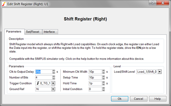
| Label | Parameter Description |
| Clock to Output Delay | Delay from the triggering clock event until the Register outputs change |
| Number of Bits | Number of input bits to the Register |
| Trigger Condition | Determines the
triggering condition of the Register clock pin:
|
| Ground Ref | Determines whether or not a device has a ground reference pin. Any digital component that has an input or output pin connected to an analog circuit node must have its Ground Ref pin connected to an analog node. This is usually the ground on the schematic. |
| Minimum Clk Width | Minimum valid clock width. Clock widths less than this parameter will not trigger the Register. |
| Setup Time | Minimum time before the triggering clock event that the input signals must remain steady so that a valid change in each input state is recognized. |
| Hold Time | Minimum time after the triggering clock event that the input signals must remain steady so that a valid change in each input state is recognized. |
| Initial Condition | Initial condition of the Register output at time=0 |
| Load/Shift Level | Determines the logic
level of the shift register load/shift ( LD/SH ) pin:
|
To define the parameters for the Set/Reset, follow these steps:
- From the Edit Shift Register (Right) dialog box, click on the Set/Reset tab.
- Make the appropriate changes to the fields described in the table below the image.
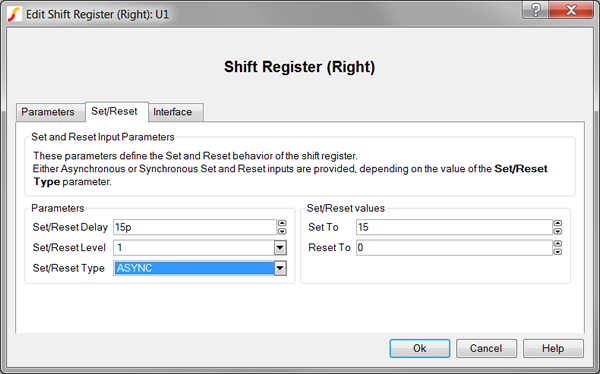
| Label | Parameter Description | ||||||
| Set/Reset Delay | Delay from when the SET or RST pin goes active until the Q output is actually set or reset. | ||||||
| Set/Reset Level | Determines the
Set/Reset level of a device:
|
||||||
| Set/Reset Type | Determines whether or
not output events are synchronized with a clock event:
|
||||||
| Set To | Determines the value of the counter output when the SET pin goes active. To set to the maximum count value, assign a value of -1. | ||||||
| Reset To | Determines the value of the counter output when the RST pin goes active. To reset to 0, assign a assign value of -1 or 0. |
To define the parameters for the interface between this digital component and each analog component connected directly to an input or output pin, follow these steps:
- From the Edit Shift Register (Right) dialog box, click on the Interface tab.
- Make the appropriate changes to the fields described in the table below the image.
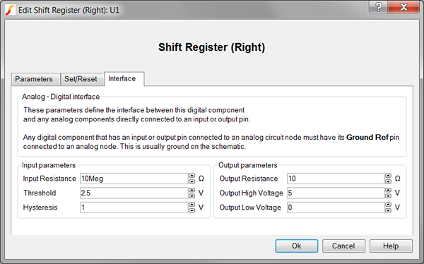
| Label | Parameter Description | |||||||
| Input Resistance | Input resistance of each Register input pin | |||||||
| Hysteresis, Threshold | 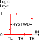 |
Hysteresis and
Threshold of the inputs. The hysteretic-window width, HYSTWD
is centered around Threshold (TH) voltage. To
determine the actual threshold ( TL , THI ),
substitute Threshold (TH) and Hysteresis
(HYSTWD) in each of the following formulas:
|
||||||
| Output Resistance | Output resistance of each Register output pin | |||||||
| Output High Voltage | Output high voltage for each Register output pin | |||||||
| Output Low Voltage | Output high voltage for each Register output pin | |||||||
Truth Tables
The truth tables below show the logic behavior with asynchronous and synchronous set/reset.
Asynchronous Set/Reset
The following truth table assumes these parameter values:
- Set/Reset Type=ASYNC
- Trigger Condition=0_TO_1 which represents a rising edge, clocked, right shift register
- Set/Reset level=1
- Load/Shift Level=Load_1/Shift_0
When the EN input is high, and the Load/Shift Level=Load_1/Shift_0, the register will load the D input when the LD/SH pin is high, and shift the Q output when the LD/SH pin is low.
| Inputs | Output | Action | |||||
| LD/SH | SET | RST | EN | D | CLK | Q | |
| 0 or 1 | 0 | 0 | 0 | 0 or 1 |
 |
Last Q | Retain state |
| 1 | 0 | 0 | 1 | 0 or 1 |
|
Data input | Load data |
| 0 | 0 | 0 | 1 | 0 |
|
Q = Last Q shifted right, MSB=0 | Shift right |
| 0 | 0 | 0 | 1 | 1 |
|
Q = Last Q shifted right, MSB=1 | Shift right |
| 0 or 1 | 1 | 0 | 0 or 1 | 0 or 1 | 0 or 1 | Asynchronous Set To value | Asynchronous set |
| 0 or 1 | 0 | 1 | 0 or 1 | 0 or 1 | 0 or 1 | Asynchronous Reset To value | Asynchronous reset |
| 0 or 1 | 1 | 1 | 0 or 1 | 0 or 1 | 0 or 1 | Last Q | Illegal concurrent ASET and ARST |
Synchronous Set/Reset
The following truth table assumes these parameter values:
- Set/Reset TypeSYNC
- Trigger Condition=0_TO_1 which represents a rising edge, clocked, right shift register
- Set/Reset level=1
- Load/Shift Level=Load_1/Shift_0
When the EN input is high and the Load/Shift Level=Load_1/Shift_0, the register will load the D input when the LD/SH pin is high, and shift the Q output when the LD/SH pin is low.
| Inputs | Output | Action | |||||
| LD/SH | SET | RST | EN | D | CLK | Q | |
| 0 or 1 | 0 | 0 | 0 | 0 or 1 |
|
Last Q | Retain state |
| 1 | 0 | 0 | 1 | 0 or 1 |
|
Data input | Load data |
| 0 | 0 | 0 | 1 | 0 |
|
Q = Last Q shifted right, MSB=0 | Shift right |
| 0 | 0 | 0 | 1 | 1 |
|
Q = Last Q shifted right, MSB=1 | Shift right |
| 0 or 1 | 1 | 0 | 0 or 1 | 0 or 1 |
|
Synchronous Set To value | Synchronous set |
| 0 or 1 | 0 | 1 | 0 or 1 | 0 or 1 |
|
Synchronous Reset To value | Synchronous reset |
| 0 or 1 | 1 | 1 | 0 or 1 | 0 or 1 |
|
Last Q | Illegal concurrent SET and RST |
Examples
The test circuit used to generate the waveform examples in the next section can be downloaded here: simplis_053_shiftregrtsoas_example.zip.
To simulate this design, follow these steps:
- Unzip the archive to a location on your computer.
- To open the schematic, double click the .sxsch file or drag that file into the SIMetrix/SIMPLIS Command Shell.
Waveforms
This example of the right shift register uses two Digital Signal Sources to generate the input pulses to the right shift register. The input source waveforms are defined in a text file with each state transition defined on a single line. These two sources excite every state transition in the Truth Table section.
For clarity, the simulation waveforms taken from the circuit example have been divided into three sections.
- Load and Shift operations when D=0: 0-1us
- Load and Shift operations when D=1: 1-2us
- Asynchronous and Synchronous Set/Reset: 2-3us
Load and Shift operations when D=0: 0-1us
The image below shows the load and shift behavior when the D input is 0. For a right shift, the D input is shifted into the MSB; since D=0, the new Q output is half the old Q. The initial condition of the right shift register is set to 15 decimal in the example.
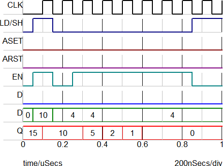
| Time | Event | Q Output |
| 100n | Load | 10 |
| 200n | Retain state | 10 |
| 300n | Shift right | 5 |
| 400n | Shift right | 2 |
| 500n | Shift right | 1 |
| 600n | Shift right | 0 |
| 700n | Shift right | 0 |
| 800n | Shift right | 0 |
Load and Shift operations when D=1: 1-2us
The image below shows the Load and Shift behavior when the D input is 1. For a Right shift the D input is shifted into the MSB, adding 2n-1 to the result. For this example, n=4, so the MSB is equal to 8.
| Time | Event | Q Output |
| 1.1u | Load | 4 |
| 1.2u | Retain state | 4 |
| 1.3u | Shift right | 10 |
| 1.4u | Shift right | 13 |
| 1.5u | Shift right | 14 |
| 1.6u | Shift right | 15 |
| 1.7u | Shift right | 15 |
| 1.8u | Shift right | 15 |
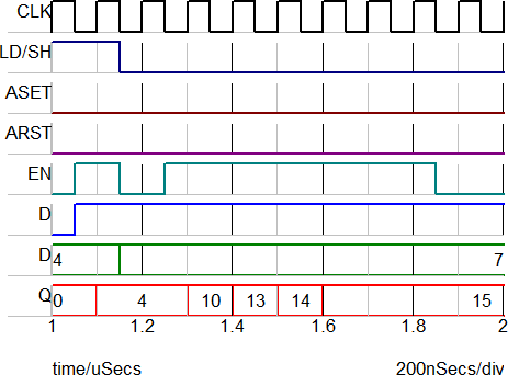
Asynchronous Set/Reset: 2-3us
The image below shows the asynchronous set/reset behavior of the register.
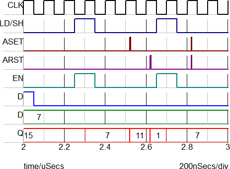
| Time | Event | Q Output |
| 2.3u | Load | 7 |
| 2.52u | Asynchronous set | 11 |
| 2.62u | Asynchronous reset | 1 |
| 2.7u | Load | 7 |
| 2.82u | Illegal concurrent ASET and ARST | 7 |
Subcircuit Parameters
Because the Shift Register (Right) model is generated by a template script when the simulation is executed, a hand-coded model cannot be inserted into a netlist. The template script for this device is simplis_make_register_model.sxscr, which licensed users can download as part of a zip archive of all built-in scripts.
To download the zip archive, follow these steps:
- Click http://www.simetrix.co.uk/simetrix80/scripts.zip to download the script archive.
- Enter the user name and password you received with your license file.
The following parameter table defines the parameters used in this model.
| Parameter Name | Label | Data Type | Range | Units | Parameter Description | |||||||
| CLK_TO_OUT_DELAY | Clock to Output Delay | Number | 1f to 1024 | s | Delay from the triggering clock event until the Register outputs change | |||||||
| GNDREF | Ground Ref | String |
|
none | Determines whether or not a device has a ground reference pin. Any digital component that has an input or output pin connected to an analog circuit node must have its Ground Ref pin connected to an analog node. This is usually the ground on the schematic. | |||||||
| HOLD_TIME | Hold Time | Number | 1f to 1024 | s | Minimum time after the triggering clock event that the input signals must remain steady so that a valid change in each input state is recognized. | |||||||
| HYSTWD, TH |
Hysteresis, Threshold |
Number | min: 1f | V | |
Hysteresis and Threshold of
the inputs. The hysteretic-window width, HYSTWD is centered around
Threshold (TH) voltage. To determine the actual threshold (
TL , THI ), substitute Threshold (TH) and
Hysteresis (HYSTWD) in each of the following formulas:
|
||||||
| IC | Initial Condition | Number |
|
none | Initial condition of the Register output at time=0 | |||||||
| LOAD_LEVEL | Load/Shift Level | Integer | none | Determines the logic level of
the shift register load/shift ( LD/SH ) pin:
|
||||||||
| MIN_CLK | Minimum Clk Width | Number | 1f to 1024 | s | Minimum valid clock width. Clock widths less than this parameter will not trigger the Register. | |||||||
| NUMBITS | Number of Bits | Integer | none | Number of input bits to the Register | ||||||||
| RESET_TO | Reset To | Number | none | Determines the value of the counter output when the RST pin goes active. To reset to 0, assign a assign value of -1 or 0. | ||||||||
| RIN | Input Resistance | Number | min: 100 | Ω | Input resistance of each Register input pin | |||||||
| ROUT | Output Resistance | Number | min: 1m | Ω | Output resistance of each Register output pin | |||||||
| SETUP_TIME | Setup Time | Number | 1f to 1024 | s | Minimum time before the triggering clock event that the input signals must remain steady so that a valid change in each input state is recognized. | |||||||
| SET_RESET_DELAY | Set/Reset Delay | Number | 1f to 1024 | s | Delay from when the SET or RST pin goes active until the Q output is actually set or reset. | |||||||
| SET_RESET_LEVEL | Set/Reset Level | Number |
|
none | Determines the Set/Reset
level of a device:
|
|||||||
| SET_RESET_TYPE | Set/Reset Type | String |
|
none | Determines whether or not
output events are synchronized with a clock event:
|
|||||||
| SET_TO | Set To | Number | none | Determines the value of the counter output when the SET pin goes active. To set to the maximum count value, assign a value of -1. | ||||||||
| TRIG_COND | Trigger Condition | String |
|
none | Determines the triggering
condition of the Register clock pin:
|
|||||||
| VOH | Output High Voltage | Number | any | V | Output high voltage for each Register output pin | |||||||
| VOL | Output Low Voltage | Number | any | V | Output high voltage for each Register output pin | |||||||