Global Start of Conversion Signals
TI Piccolo™ ePWM
SystemDesigner includes a high-level PWM module based on the TI Piccolo™ ePWM. One of the powerful features of the ePWM is the ability to generate start-of-conversion (SOC) signals, SOCA and SOCB, at any point in the PWM period. The SOC signals are then routed to the analog-to-digital converters in the design and are used to sample voltages or currents at the SOC time instants.
The SystemDesigner architecture automatically routes the SOCA and SOCB signals from the ePWM blocks to the ADCs without any visible wiring. You can download a circuit example that demonstrates this from here.
- The ePWM is configured to have a 100kHz switching frequency with a trailing edge modulation scheme.
- The period register, TBPRD, is set to 499; and the System Clock is 50MHz.
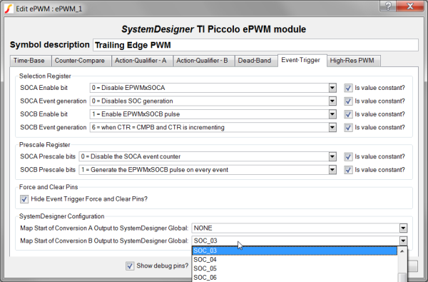
- The ePWM is configured to create SOCB events when the timebase
counter equals CMPB. These SOCB outputs are routed from the ePWM to
the ADC through the global SOC channel 'SOC_03'.
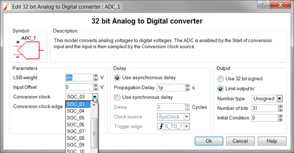
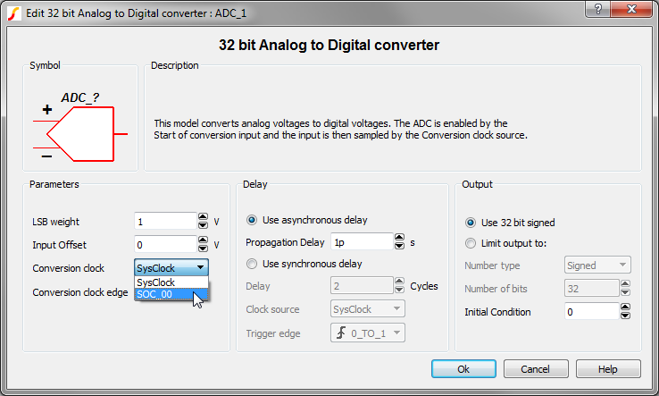
- The ADC converter then uses this SOC signal to convert the analog
voltage to a digital value every start of conversion event. You set
the ADC to use the SOC_03 signal for the SOCB output on the ADC dialog:
- Once the ePWM is generating SOC signals and the ADC is receiving
the signals, you can examine the rest of the circuit, pictured here.
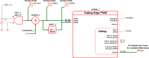
The table below describes the design:
| Schematic Component | Description |
| V1 | A 1V peak ( -1V to +1V ) sine wave source |
| ADC1 | An ADC which quantizes the input voltage with 2mV LSB weight. The output is limited to 0 |
| CONSTANT_1 | A 2 LSB constant offset |
| ADDER_1 | Adds the 2 LSB offset to the ADC output and applies this value to the ePWM CMPA input |
| SHIFT_1 | Divides the CMPA by 2, applying the result to the ePWM CMPB input |
| ePWM_1 | Generates trailing edge PWM patterns based on the CMPA bus and also generates SOCB pulses when the count value reaches the CMPB input bus |
Starting at the left side of the schematic, the sine wave voltage source V1 is input to the ADC. This sine wave has a maximum value of 1V and a minimum value of -1V. The ADC then quantizes this voltage into a 2mV LSB. Ordinarily, when the analog input is negative, the ADC output would become negative, but in this case the ADC limits its output to unsigned integers with 31 bits of resolution, which means that the output of the ADC is never less than zero.
The constant and the adder ensure that the output of the shift block, the CMPB input, is never zero. This also means the ePWM has a minimum pulse width of 2/600 or approximately 0.33%.
The ePWM has two inputs: CMPA and CMPB with CMPB=0.5*CMPA. The CMPA input sets the pulse width, and the CMPB input sets the SOCB generation. Since the CMPB input is always half the CMPA input, the SOCB signal is generated midway through the PWM ON time. In many switch-mode power converters, sampling midway through the ON time captures the average value of the signal. Capturing that average value often helps to eliminate any peak-to-average error in the samples.
The integer-sampled data simulation results are shown below.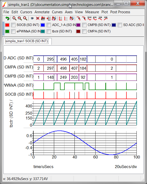
* Piccolo is a trademark of Texas Instruments Incorporated.
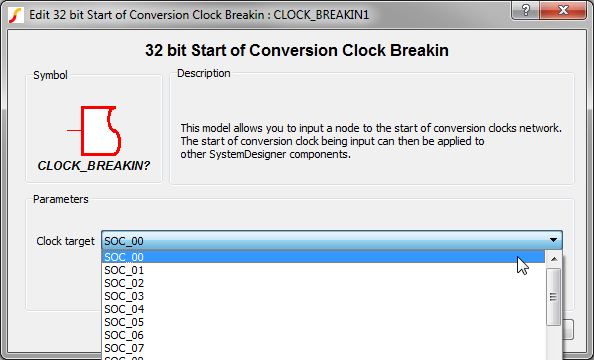
Start of Conversion Clock Breakin
Along with
the TI Piccolo™ ePWM, an SOC signal can be generated by a node within the schematic. The
SystemDesigner architecture automatically routes the input signal from the SystemDesigner Start of Conversion Clock Breakin to the rest of
the SystemDesigner components without any visible wiring. You can download a circuit example that
demonstrates this from here. 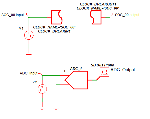
A brief description of the example circuit is as follows:
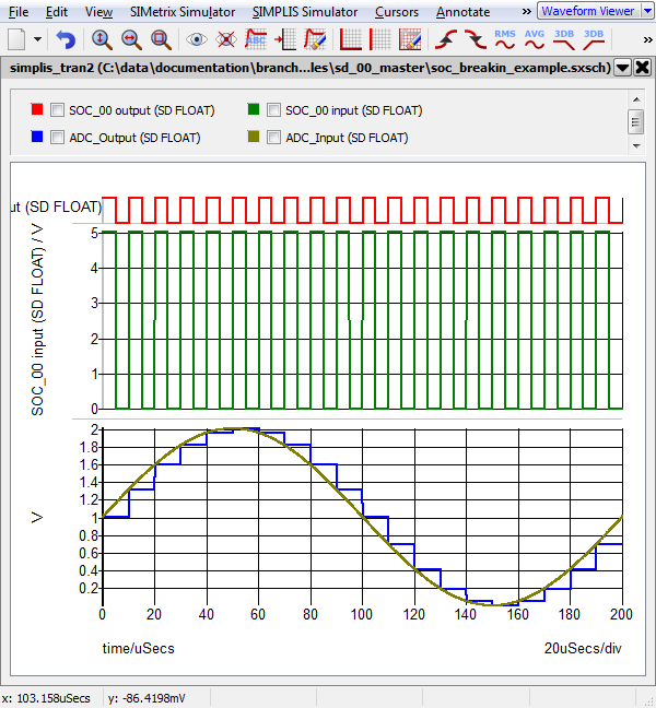
- The waveform generator V1 connected to the SOC Clock Breakin CLOCK_BREAKIN1 is configured to output a 100kHz square wave.
- The waveform generator V2 connected to the ADC is configured to output a 5kHz sine wave.
- The SOC Clock Breakin is configured to route the input clock to the global SOC
channel 'SOC_00' Note: a start of conversion clock can be set by only one SOC Clock Breakin or ePWM. If a channel is being set by another device, it will not appear in the dialog.
- The ADC's conversion clock is set to 'SOC_00' and the LSB weight is set to 1V.
The double precision floating point-sampled data simulation results are shown below.