SIMPLIS MOSFET Models
Any SPICE MOSFET model installed in the SIMetrix library can be converted for use in SIMPLIS. When a MOSFET is placed on a SIMPLIS schematic, a model parameter extraction routine is invoked to automatically convert the SPICE model to a SIMPLIS model. During the model parameter extraction process, SIMetrix/SIMPLIS automatically runs several SPICE simulations on the SPICE model and extracts the SIMPLIS model parameters. After the Piecewise Linear (PWL) model parameters have been extracted, the resulting MOSFET model will run in SIMPLIS.
In this topic:
Extracting the MOSFET Parameters
When you place a MOSFET symbol on a schematic, the Extract MOSFET Parameters dialog opens for you to edit the default test conditions. You should change the test conditions to accurately reflect the expected voltage, current, and temperature of the device in your circuit.
The default test conditions are defined using the command shell menu, . For additional information, see SIMPLIS MOSFET Options.
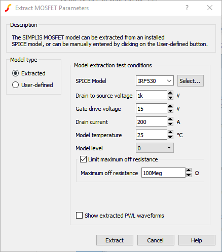
The following table describes the Extract MOSFET Parameters dialog test conditions.
| Test Condition | Default Value | Units | Description |
| SPICE Model | IRF530 | The SPICE model used to extract SIMPLIS parameters. | |
| Model type | Extracted | Invokes the model parameter extraction algorithms. |
| Drain to source voltage | 1k | V | The peak off-state voltage seen by this device. Used to extract capacitance for model levels which include parasitic capacitance. Breakdown is not modeled. |
| Gate drive voltage | 15 | V | Gate to source voltage to extract RDS(on). |
| Drain Current | 200 | A | Peak drain current to extract the RDS(on) and forward gain of the MOSFET. |
| Model temperature | 25 | °C | Temperature used for all extraction simulations. |
| Model level | 0 | Model complexity. For information on choosing the model level, see MOSFET Model Levels. | |
| Limit maximum off resistance | Checked | none | Limits the off resistance for the MOSFET. For some SPICE models, this will produce a SIMPLIS model which runs faster. |
| Maximum off resistance | 100Meg | W | The maximum off resistance of the MOSFET switch. This value is used only if "Limit maximum off resistance" is checked. |
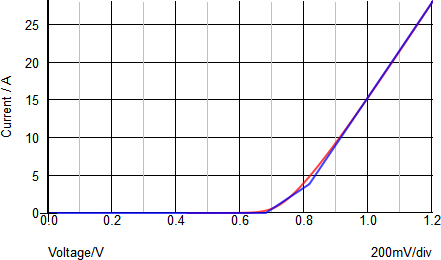
Show extracted PWL waveforms option
Beginning in version 8.2, there is now an option to plot the extracted parameters as a set of PWL curves. To enable this option, select the Show extracted PWL waveforms checkbox and extract the model. After the model is extracted, a set of curves will be generated comparing the extracted PWL curves against the simulated SPICE curves. The curves displayed will depend on the model level being extracted.
Below is a typical PWL approximation of the Forward Bias Current characteristic of the MOSFET's body diode, with the SPICE curve in red and the PWL curve in blue.
SIMPLIS MOSFET Model Levels
The SIMPLIS MOSFET models have multiple levels to balance simulation speed vs. model accuracy. There are currently four levels: 0, 1, 2, and 3. As the model level increases, so does the model complexity and, as a rule, simulation times also increase.
SIMPLIS extracts a model based on the model level chosen in the Extract MOSFET Parameters dialog. Currently model levels 0, 1, and 2 are supported by the model parameter extraction algorithms. The level 3 model is intended for more detailed modeling and can be manually generated from a device datasheet or from a spreadsheet or other program. For details of the Level 3 model, see Manually Generate and Customize MOSFET Models. Although these models are internally saved as ASCII text, the following illustrations show the three model levels in a schematic form.
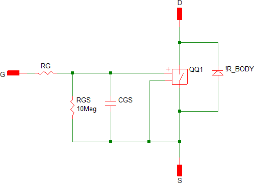
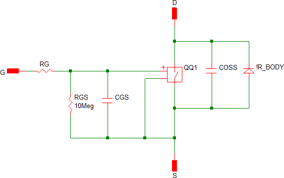
Level 0 Model
Level 0 models a switch with on/off resistance values, a body diode, gate resistance, and gate-to-source capacitance. The Level 0 Model can be used for AC Bode Plots and for simulating output voltage during load and line transients when the actual switching waveform shapes are not critical.
- The conduction region is modeled with an on and off resistance.
- CGS capacitance is modeled with a linear capacitor and has a parallel 10Meg resistor.
- Gate resistance is modeled with RG.
- The body diode is modeled with a 2- or 3-segment resistor; the number of segments is specified in the SIMPLIS Options dialog.
- There is no output (CDS) or reverse capacitance (CDG).
Below is a schematic view of a Level 0 model:
| Level 0 models these circuit elements | Level 0 Schematic | ||||||||||
|
|
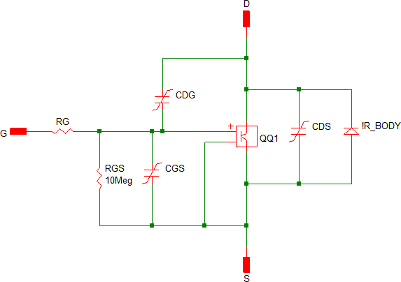
Level 1 Model
Level 1 models a switch with on/off resistance values, a body diode, gate resistance, gate-to-source capacitance, plus a lumped-linear Coss capacitance across drain and source terminals. The Level 1 Model can be used for power stage simulations, including Quasi-resonant, LLC, and phase-shifted bridge topologies,as well as for AC Bode Plots and for simulating output voltage during load and line transient.
- The conduction region is modeled with an on and off resistance.
- CGS capacitance is modeled with a linear capacitor and has a parallel 10Meg resistor.
- Gate resistance is modeled with RG.
- The body diode is modeled with a 2- or 3-segment resistor; the number of segments is specified in the SIMPLIS Options dialog.
- There is no reverse capacitance (CDG).
- The bulk COSS capacitor is the parallel CDG and CDS capacitors with the value as
follows:
COSS = (QCDS1 - QCDS0)/(VCDS1 - VCDS0)
Below is a schematic view of a Level 1 model:
| Level 1 models these circuit elements | Level 1 Schematic | ||||||||||||
|
|
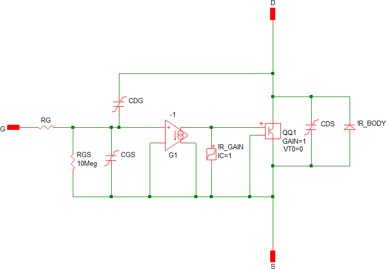
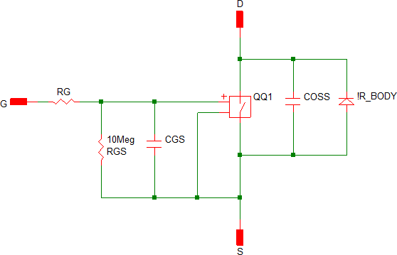
Level 2 Model
Level 2 models a switch with forward transconductance gain, a body diode, and gate-to-source capacitance, plus a nonlinear Gate-Drain, Drain-Source, and Gate-Source capacitors. The active region is modeled by a linear transconductance gain (ID is proportional to VGS - VT0). The Level 2 Model can be used for switching losses, MOSFET voltage and current stresses, and all simulations covered by Level 0 and Level 1 models.
- Forward conduction is modeled with a two-segment gain. The following gain information assumes that the device is being switched from an off state to an on state:
-
- Below the threshold voltage (VT0 - HYSTWD/2)), the gain is 0.
- Above the threshold, the gain is GAIN = ID2/(VGS2 - VT0 - HYSTWD/2) units: A/V (transconductance)
- Gate resistance is modeled with RG.
- The body diode is modeled with a 2- or 3-segment resistor; the number of segments is specified in the SIMPLIS Options dialog.
- This model level implements non-linear capacitors for all three capacitors (CGS ,
CDG and CDS). The Model Extraction algorithms determine the number of segments for
each capacitor. Typically the Gate-Source capacitor is linear, while the
Drain-Gate and Drain-Source capacitors have four segments. Note: The actual capacitor used is determined by the CGS_NSEG , CDG_NSEG and CDS_NSEG parameters.
-
- If one of these parameters is set to 0, the capacitor at that location will be an open circuit.
- If the number of segments is set to 1, a linear capacitor is implemented
with capacitance:
Cxx = (Qxx1 - Qxx0)/(Vxx1 - Vxx0)
where "xx" is the capacitor GS, DG, or DS. - Otherwise, if the CXX_NSEG parameter is set to a value greater than 1, the capacitor is implemented with a PWL capacitor. For more information, see Capacitor Models section below.
Below is a schematic view of Level 2 model:
| Level 2 models these circuit elements | Level 2 Schematic | ||||||||||||||
|
|
Level 3 Model
The Level 3 model extends the Level 2 model to include up to 5 forward transconductance gain segments. The Level 3 model can be used to more accurately model converter losses for converters which operate over a wide range of currents.
- The level 3 model is the same as the Level 2 model but the Forward Conduction is modeled with a variable number of PWL segments.
- As with the Level 2 model, the first segment has a gain of 0.
- The second segment has a gain of GAIN2 = ID2/(VGS2 - VT0) units: A/V (transconductance)
- Further segments have gain values which are defined by the slopes between successive point pairs. For example, the third segment has a gain of GAIN3 = (ID3 - ID2)/(VGS3 - VGS2) units: A/V (transconductance)
- Up to five segments of gain can be used with this model. The number of gain segments is controlled by the GAIN_NSEG parameter.
Below is a schematic view of a Level 3 Model:
| Level 3 models these circuit elements | Level 3 Schematic | ||||||||||||||||||
|
|
User-defined Models
The user-defined model uses parameters entered directly in the Edit MOSFET Parameters dialog without invoking the model extraction algorithms. A MOSFET can be switched from an extracted model to a user-defined model at any point; however the extracted parameters are by default copied over to the user-defined parameters, replacing any user-entered values. You can disable this behavior in the SIMPLIS Options dialog by clearing the check box labeled "Automatically copy extracted parameters to User-defined parameters." You can access these options from the command shell menu . For more information, see SIMPLIS MOSFET Options.
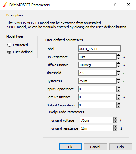
The following table describes the Edit MOSFET Parameters entries for a User-defined model.
| Parameters | Default Value | Units | Description |
| Label: | USER_LABEL | Any descriptive text. Cannot contain white space characters. | |
| Model type | User-defined | The values in this dialog are used literally. | |
| On Resistance: | 10m | Ω | The on resistance of the MOSFET switch. |
| Off Resistance: | 100Meg | Ω | The off resistance of the MOSFET switch |
| Threshold: | 2.5 | V | MOSFET threshold voltage -
the MOSFET will turn on at (Threshold + 1/2 Hysteresis). Turn off occurs at (Threshold - 1/2 Hysteresis). |
| Hysteresis: | 250m | V | The hysteresis of the MOSFET |
| Input Capacitance: | 0 | F | The input capacitance ( CGS) of the MOSFET. Set to 0 to remove the capacitor from the model. |
| Gate Resistance: | 0 | W | The internal resistance of the MOSFET. Set to 0 to remove the gate resistance from the model. |
| Output Capacitance: | 0 | F | A non-zero value will place a
linear capacitance between the MOSFET drain and source terminals. Set to 0 to remove capacitor from the model. |
| Body Diode Parameters | |||
| Forward voltage: | 750m | V | Diode forward voltage drop. The diode effectively turns on at this voltage. |
| Forward resistance: | 10m | Ω | The Body Diode resistance at voltages higher than the Forward voltage |
User-defined model schematic
| Models these circuit elements | User-defined Schematic | ||||||||||||
|
|
Customize or Manually Generate MOSFET Models
You can customize or manually generate your own MOSFET models using a parameter string with multiple PARAM_NAME=PARAM_VALUE key-value pairs. The parameter names and their functions are described in the MOSFET Model Parameters section below. You can interpret the SIMPLIS parameter values from device datasheet specifications and curves.
You can compose the parameter string in a text editor, spreadsheet, or script. The order of the parameter names in the parameter string and the capitalization of the parameter names are irrelevant.
You can include a PROTECTED=1 key-value pair to prevent from extracting a model and overwriting your manually generated parameters. The PROTECTED=1 key-value pair is not used in the simulation.
To customize or generate your own MOSFET model, follow these steps:
- Create a parameter string of multiple PARAM_NAME=PARAM_VALUE key-value pairs using your preferred text editor, spreadsheet or script.
- Add the PROTECTED=1 key-value pair to the parameter string.
- Extract a MOSFET model and place it on a schematic.
- Right click on the symbol and select Edit/Add Properties....
- Double click on the PARAM_VALUES property.Result: The Edit Property dialog opens. At this point, you can change individual parameters in the Value box, or replace the entire default properties with the parameter string that you created in Step 2.
- To replace the entire string, follow these steps:
- Click in the Value box and type Ctrl A to select all of the existing parameter string, and press Delete.
- Copy the parameter string you completed in Step 2 and paste into the Value box.
- Click Ok.
- To change the name of your customized model, double click the VALUE property in the Edit Properties dialog, and change the name in the Value box.
- To return to the schematic, click Ok.
prop PARAM_VALUES parameter_stringwhere parameter_string is the set of key-value pairs that you created in Steps 1 and 2 above.
MOSFET Model Parameters
The following tables detail the parameters which define the electrical behavior of the MOSFET model. Several other parameters in the PARAM_VALUES property have no effect on the electrical behavior of the model. These parameters are used to populate the Extract MOSFET Parameters dialog box.
| Parameter Name | Default Value | Description |
| LEVEL | 0 | Model Level |
| RDSON | 10m | Switch QQ1 On resistance |
| ROFF | 100Meg | Switch QQ1 Off Resistance |
| VT0 | 2.5 | Switch QQ1 Threshold |
| HYSTWD | 1 | Switch QQ1 Hysteresis |
| RG | 1.123456789 | Gate Resistance |
| Parameter Names | Default Value | Description | |
| GAIN_NSEG | 2 (off and on) | Number of segments in the Gain model | |
| VT0 | 1.123456789 | X-Y point definitions for
gain:
|
|
| VGS2 | ID2 | 1.123456789 | |
| VGS3 | ID3 | 1.123456789 | |
| VGS4 | ID4 | 1.123456789 | |
| VGS5 | ID5 | 1.123456789 | |
| Parameter Names | Default Value | Description | |
| BD_NSEG | 3 | Number of segments in the
body diode model.
|
|
| VD0 | IBD0 | 1.123456789 | X-Y point definitions for
body diode:
|
| VD1 | IBD1 | 1.123456789 | |
| VD2 | IBD2 | 1.123456789 | |
| VD3 | IBD3 | 1.123456789 | |
| VD4 | IBD4 | 1.123456789 | |
| VD5 | IBD5 | 1.123456789 | |
| VD6 | IBD6 | 1.123456789 | |
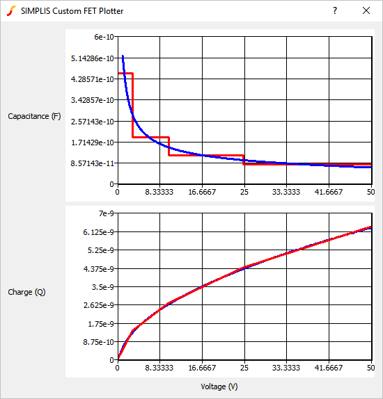
Capacitor Models
Capacitors are modeled in SIMPLIS with Piece-Wise Linear capacitors.
- A system of point-pairs is used with the X-Y plane defined with Voltage on the X-axis and Charge on the Y-axis.
- A system of subscripts is used to define the point pairs. For example, VCDS0 and QCDS0 represent the lowest Voltage-Charge pair for the CDS capacitor with increasing subscripts representing increasing VDS voltages.
- On the Voltage-Charge plane, the capacitance is the slope of any segment.
- The actual number of segments is controlled by the CXX_NSEG, where "xx" is the capacitor GS, DG, or DS. The model uses only the number of point-pairs defined by CXX_NSEG; higher numbered point-pairs ignored.
| Parameter Names | Default Value | Description | |
| CGS_NSEG | 1 | Number of segments in the Gate-Source capacitor model | |
| VCGS0 | QCGS0 | 1.123456789 | X-Y point definitions
for CGS:
|
| VCGS1 | QCGS1 | 1.123456789 | |
| VCGS2 | QCGS2 | 1.123456789 | |
| VCGS3 | QCGS3 | 1.123456789 | |
| VCGS4 | QCGS4 | 1.123456789 | |
| VCGS5 | QCGS5 | 1.123456789 | |
| VCGS6 | QCGS6 | 1.123456789 | |
| VCGS7 | QCGS7 | 1.123456789 | |
| VCGS8 | QCGS8 | 1.123456789 | |
| VCGS9 | QCGS9 | 1.123456789 | |
| VCGS10 | QCGS10 | 1.123456789 | |
| Parameter Names | Default Value | Description | |
| CDS_NSEG | 4 | Number of segments in the Drain-Source capacitor model | |
| VCDS0 | QCDS0 | 1.123456789 | X-Y point definitions
for CDS:
|
| VCDS1 | QCDS1 | 1.123456789 | |
| VCDS2 | QCDS2 | 1.123456789 | |
| VCDS3 | QCDS3 | 1.123456789 | |
| VCDS4 | QCDS4 | 1.123456789 | |
| VCDS5 | QCDS5 | 1.123456789 | |
| VCDS6 | QCDS6 | 1.123456789 | |
| VCDS7 | QCDS7 | 1.123456789 | |
| VCDS8 | QCDS8 | 1.123456789 | |
| VCDS9 | QCDS9 | 1.123456789 | |
| VCDS10 | QCDS10 | 1.123456789 | |
| Parameter Names | Default Value | Description | |
| CDG_NSEG | 4 | Number of segments in the Drain-Gate capacitor model | |
| VCDG0 | QCDG0 | 1.123456789 | X-Y point definitions
for Drain-Gate capacitor:
|
| VCDG1 | QCDG1 | 1.123456789 | |
| VCDG2 | QCDG2 | 1.123456789 | |
| VCDG3 | QCDG3 | 1.123456789 | |
| VCDG4 | QCDG4 | 1.123456789 | |
| VCDG5 | QCDG5 | 1.123456789 | |
| VCDG6 | QCDG6 | 1.123456789 | |
| VCDG7 | QCDG7 | 1.123456789 | |
| VCDG8 | QCDG8 | 1.123456789 | |
| VCDG9 | QCDG9 | 1.123456789 | |
| VCDG10 | QCDG10 | 1.123456789 | |
MOSFETs From Datasheets
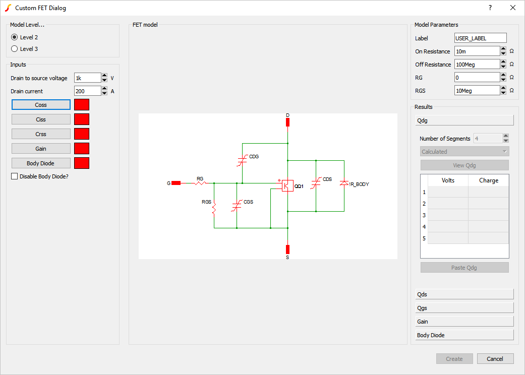
Beginning in version 8.3, datasheet waveforms can be used to create or customize a SIMPLIS MOSFET model.
Creating a new MOSFET using a datasheet
To create a SIMPLIS MOSFET model using a datasheet, open the Part Selector and choose or depending on desired MOSFET type. The resulting dialog will appear:
Customizing an extracted MOSFET using a datasheet
To customize a SIMPLIS MOSFET after Extracting the MOSFET Parameters, right click on the MOSFET symbol, and select Edit Additional Parameters... menu item. The resulting dialog will appear:
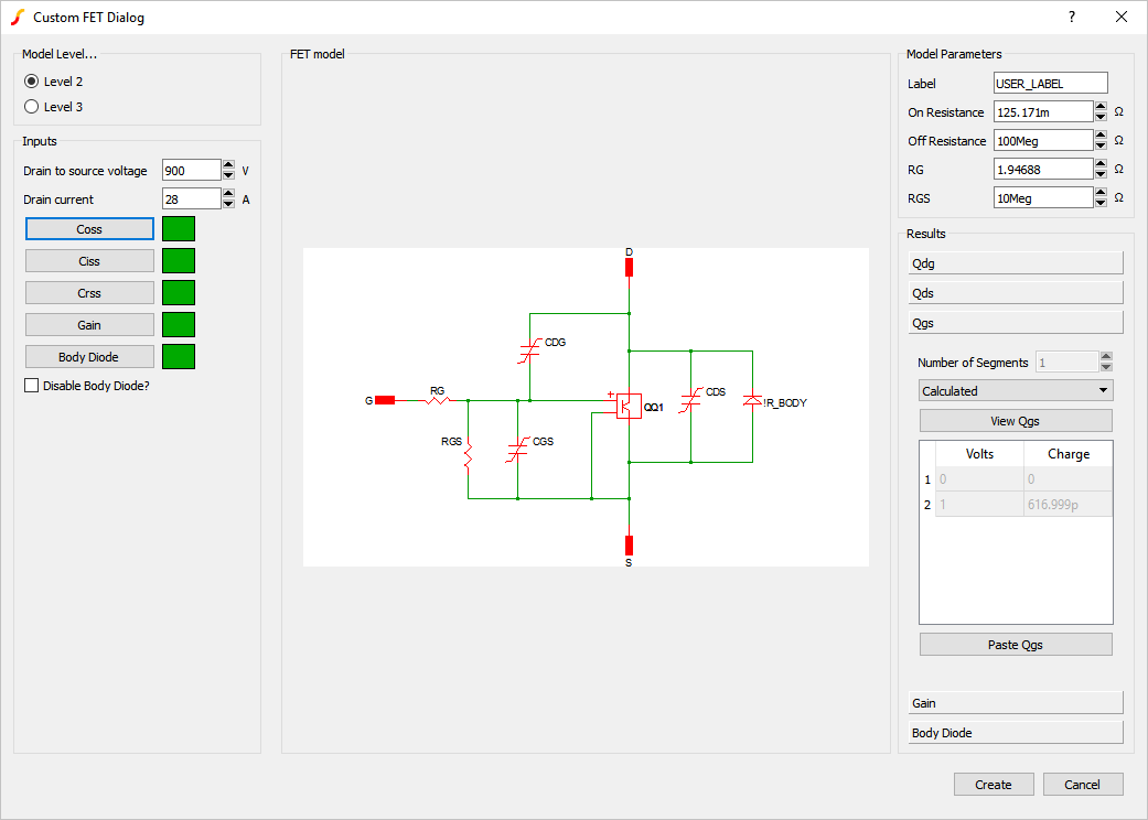
Using the Dialog
The dialog works in a left-to-right fashion. Starting with the Model Level... where a Level 2 or Level 3 model can be selected.
The entries in the Inputs section are used to create the PWL definitions.
| Entry Names | Default Value | Description |
| Drain to source Voltage | 1k | The peak off-state voltage seen by this device. Used to extract capacitance. Breakdown is not modeled. |
| Drain current | 200 | Peak drain current to extract the forward gain of the MOSFET. |
| Coss | n/a | Select to digitize the Coss datasheet waveform. |
| Ciss | n/a | Select to digitize the Ciss datasheet waveform. |
| Crss | n/a | Select to digitize the Crss datasheet waveform. |
| Gain | n/a | Select to digitize the Transconductance datasheet waveform. |
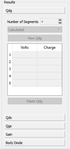
| Body Diode | n/a | Select to digitize the Body Diode Forward Voltage characteristics datasheet waveform. |
| Disable Body Diode? | Unchecked | Select to omit the Body Diode from the model. |
The entries in the Model Parameters section are not used to create the PWL definitions and are passed in to the MOSFET subcircuit.
| Entry Names | Default Value | Description |
| Label | USER_LABEL | A Label to describe the device. The label may only include alpha-numeric characters and the underscore character. The actual text is only used for describing the device, and is not used in simulation. |
| On Resistance | 10m | The on resistance of the MOSFET switch. |
| Off Resistance | 100Meg | The off resistance of the MOSFET switch. |
| RG | 0 | The gate resistance of the MOSFET. |
| RGS | 10Meg | The gate-to-source resistance of the MOSFET. |
Pressing the View button will plot the calculated and PWL characteristics.