3.3 Set up an AC Analysis
You are now ready to set up the buck converter for an AC analysis. You first will add a basic pulse width modulator (PWM) to the circuit.
In this topic:
Key Concepts
This topic addresses the following key concepts:
- The SIMPLIS AC analysis simulates the time-domain, switching circuit model, no averaged model is needed.
- Although you could run an AC analysis on the schematic as it is, the AC analysis would have no additional information because the schematic has no modulator.
- Version 8.0 has a Multi-Level gate driver which can represent several kinds of gate drivers and will be used in this design. The driver symbol dynamically changes when you change the model level, depicting the model.
- You can search for symbols using the
 tool button.
What You Will Learn
In this topic, you will learn the following:
- How to add a basic PWM modulator, MOSFET gate driver and a AC small signal source.
- How to set the analysis directives and run a POP and AC analysis on the converter.
Getting Started
For this exercise, you can use the last schematic you saved or you can open 4_SIMPLIS_tutorial_buck_converter.sxsch.
If the grid is not showing, go to the menu bar in the schematic editor, and select .
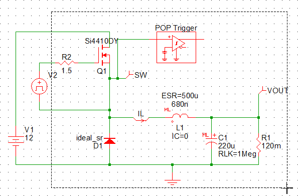
3.3.1 Prepare the Schematic
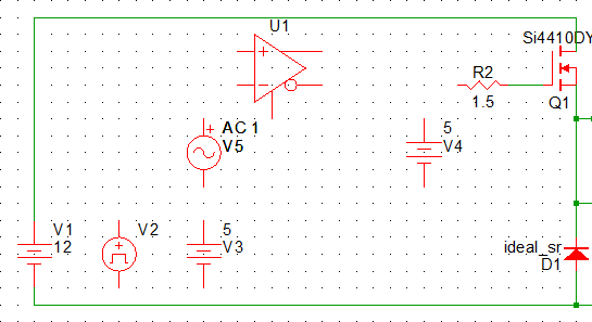
To make room for the new modulator symbols, you will need to move several symbols on the previously saved schematic
To move the symbols, follow these steps in the schematic editor:
- Open the schematic that you saved after running the POP simulation
or
open 4_SIMPLIS_tutorial_buck_converter.sxsch. - To select components to move to the right, place the cross hair at the top of the
window between the V2 and R2 components and draw a box around all of
the components to the right as shown below:
 Result: The selected components change from red to blue.
 - Place the cross hair on any blue line, and drag the selected components 20 grid points to the right.
- To delete each of the four wires highlighted in blue below, place the cross hair on
the wire, click the left mouse button, and then type Ctrl+X or press
Delete.
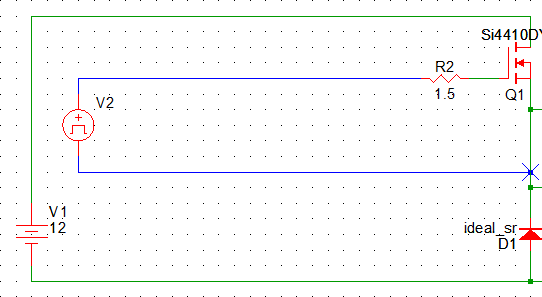
- Click the V2 symbol and drag it to the right two grid points and down so it
is even with V1 as shown below:
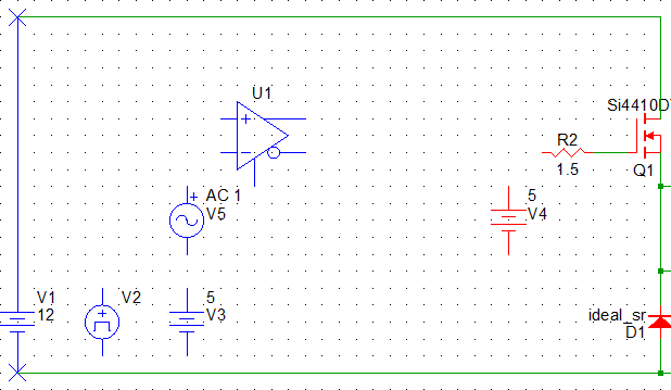
3.3.2 Add the New Symbols
To add two power supplies and an AC source, follow these steps:
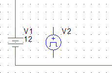
- From the Commonly Used Parts category, double click Power Supply.
- Move the cross hair to the right of the waveform generator V2, and click the
left mouse button to place V3 as shown below.
 Result: This voltage source V3 will be the duty cycle control for the power supply.
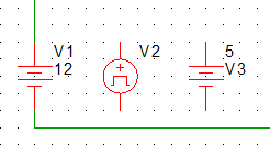
 - Repeat step 1 and place the cross hair above and to the left of D1 and then
click the left mouse button to place V4 as shown below.
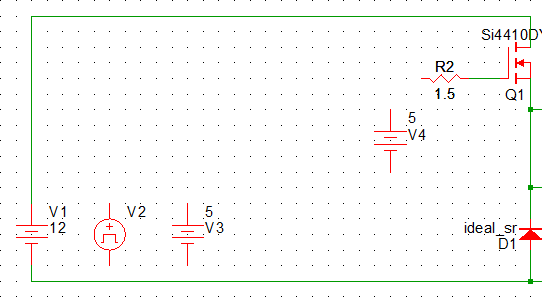 Result: V4 will be the floating gate drive power supply.
 - In the Commonly Used Parts category, double click AC source (for AC
analysis); place the cross hair above the V3 symbol, and click to place
the AC source as shown below.
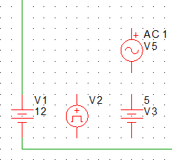 Result: This AC source V5 will perturb the circuit during the AC analysis.
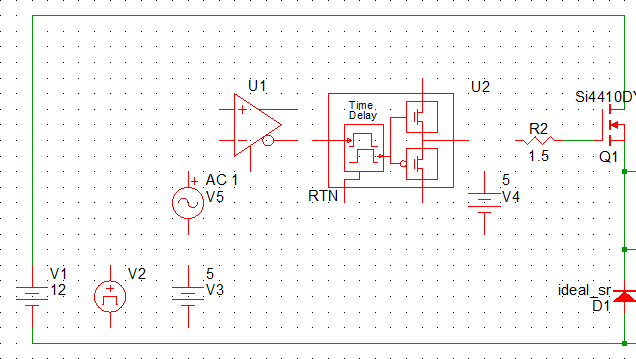
To place the Comparator and move some of the symbols, follow these steps:
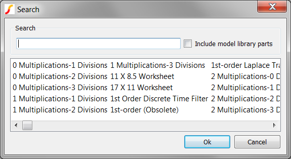
- From the toolbar, find the tool button with the binocular icon . Click on the tool button to open the Search dialog.Result: The Search dialog opens.
 Note: You can also open the Search dialog with the menu item.
 - Enter com in the search field.Result: The symbols which contain the sub-string com are shown.
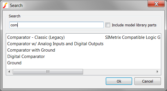
- Select the Comparator - Classic (Legacy) entry and click Ok.
- Place the cross hair just to the right of V4 so that the negative input and
inverted output line up with the R2 symbol, and click the left mouse button to
palce the comparator U1 as shown below.
 Result: U1 in conjunction with the ramp source V2 will form the duty-cycle modulator, with V3 providing a duty cycle input.
 - Click the line just above the U1 symbol text and drag the mouse to move it up 4 grid points.
- Hold down the left mouse button and draw a box around all of the symbols on the left
side (V1, V2, V3, V5, and U1), and then drag them
all to the left 6 grid points.
The next symbol for this design is the Version 8.0 Multi-Level MOSFET driver.
To place a multi-level MOSFET driver, follow these steps:
- In the Part Selector, double click the MOSFET Drivers category and then double click Multi-Level MOSFET Driver (Version 8.0+).
- Place the cross hair between the comparator U1 and the resistor R2.
- Click the left mouse button to place the new symbol as shown below.
Finally, you need a probe to generate the gain and phase curves. To add a Bode Plot probe, follow these steps:
- From the Commonly Used Parts category, double click Probe- Bode Plot -
Gain/Phase - w/ Measurements, and move the cross hair to the top of the
schematic above the POP Trigger symbol and then click to place it on the grid.
 Result: A dialog opens for you to add common measurements to this Bode Plot probe.
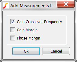
- Uncheck Gain Margin and Phase Margin, leaving only Gain Crossover Frequency
checked, and then click Ok.Result: The built-in Gain Crossover Frequency measurement is added to the probe. This measurement will be made every time the simulation is run.
3.3.3 Add Wiring to the Schematic
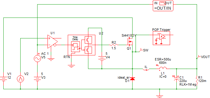
Use the following diagram to add the wiring to your schematic. You will need to add ground symbols to the ground returns of U1 and U2. The keyboard shortcut G places ground symbols.
3.3.4 Save your Schematic
To save your schematic, follow these steps:
- Select .
- Navigate to your working directory where you are saving your schematics.
- Name the file 5_my_buck_converter.sxsch.
3.3.5 Change Parameter Values
With the additional symbols, you have repurposed the waveform generator V2 from the pulse source to the modulator ramp voltage source. In the procedure below, you will set the modulator ramp to 1V peak-peak so that when the DC source (V3) has a DC value of 0.11V, the duty cycle will be 11%.
To change the parameter values for the waveform generator, follow these steps:
- Double click the V2 symbol.Result: The Edit Waveform dialog box opens.
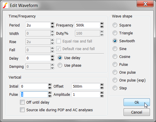
- On the right side of the dialog in the Wave shape section, select the Sawtooth radio button.
- Set the Pulse value to 1V.
- Click Ok.
- Double click the V3 symbol and change its DC Voltage to 110mV; and then click Ok.
To change values on the MOSFET driver, follow these steps:
- Double click on U2, the Multi-Level MOSFET Driver.
- Change the Model level to 0.
- Uncheck the Use delay checkbox.
- Click Ok.Result: The symbol for the MOSFET driver changes to represent the level 0 driver which uses on/off resistance switches to drive the MOSFET. Additionally, the delay block has been removed from the symbol indicating that the driver has zero delay.
3.3.6 Setup and Run an AC Analysis
To run an AC analysis, follow these steps:
- From the menu bar in the Schematic editor, select .
- On the right side of the dialog box, click to check AC as shown below.
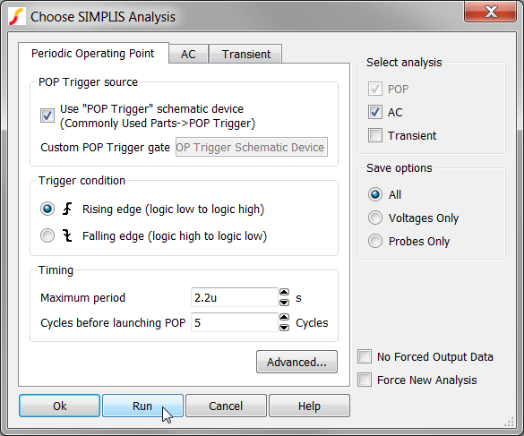 Note: The POP check box is also selected and grayed out indicating that both POP and AC analyses are to be performed. For every AC simulation, SIMPLIS requires a POP simulation to be run first.
 - Click Run.
or
Click Ok and then press F9 .Result: The control to output response of the buck converter is output to the waveform viewer.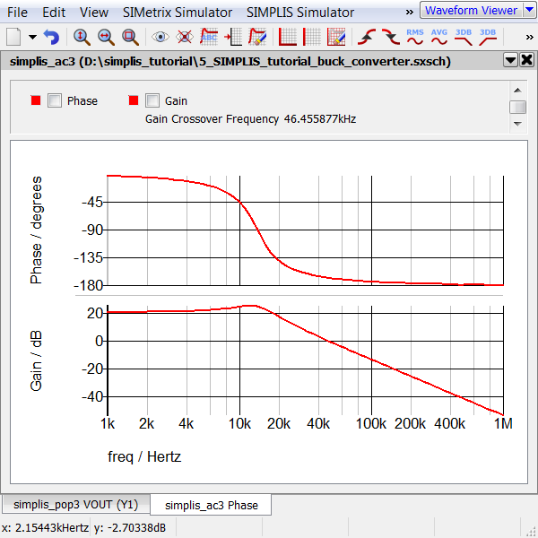
Notice that the Gain Crossover Frequency is measured and displayed on the Gain curve legend at the top of the box. In this context the Gain Crossover Frequency is simply the frequency where the Gain reaches 0dB. As expected the Gain at low frequency is slightly greater than 20dB, and the control-to-output transfer function has a double pole at the LC frequency of approximately 12.5kHz.
It is important to note that the AC response of this circuit is taken from the full, non-linear switching model, and no small signal AC model is required. As a result, the effects of parasitic elements in the design are accurately modeled and automatically included in the AC analysis. A simple example is the DC gain of the power stage. The DC gain is slightly lower than the predicted value due to losses in the circuit.
3.3.7 Save your Schematic
To save your schematic, follow these steps:
- From the menu bar, select .
- Navigate to your working directory where you are saving your schematics.
- Name the file 6_my_buck_converter.sxsch.
A schematic saved at this state can be downloaded here: 6_SIMPLIS_tutorial_buck_converter.sxsch.
In the chapter 4, you will separate the POP waveforms to make it easier to understand the converter operation and performance.