5.3 Creating Hierarchical Schematics
In section 5.2 Set up a Load Transient Simulation, you modified the schematic to run a pulse load test on the complete closed loop converter. The schematic completed in that section is large and difficult to navigate. A natural progression is to add a level of hierarchy - that is, modify the schematic to use sub-blocks, or child components,with each sub-block representing some portion of the circuit, like the compensator.
SIMetrix/SIMPLIS has an easy-to-use system for dividing schematics into sub-blocks. Each sub-block is called a Schematic Component and is saved as an individual file containing both the schematic and the symbol representing that sub-schematic. In this section you will create a schematic component out of the compensator portion of the schematic.
In this topic:
Key Concepts
The following key concepts are addressed in this section:
- Module ports define the electrical connections from the sub-schematic to the parent schematic.
- Schematic component files are containers similar to schematics but with an additional space reserved for the symbol.
- Symbols can be auto created by SIMetrix/SIMPLIS.
- After circuit blocks are divided into a hierarchy, you can create a truly modular design by swapping blocks that have common functionality and a common symbol. The hierarchical compensator block you create in this topic can also easily be used in other models.
What You Will Learn
In this section of the tutorial, you will learn the following:
- How to add module ports to schematics.
- How to automatically create symbols for hierarchical components which connect to those module ports.
- How to edit symbols using the symbol editor.
5.3.1 Create a Hierarchical Schematic Component From the Compensator
Creating a hierarchical block out of a working schematic requires three major steps:
- Adding module ports to the schematic to identify which nodes connect to other blocks.
- Saving the schematic as a schematic component file.
- Creating a symbol which has pins corresponding to the underlying module ports.Note: An automated system exists to generate symbols for schematic components.
To get started, you will need the schematic from the last section. You can download a schematic at this stage here: 12_SIMPLIS_tutorial_buck_converter.sxsch.
To add the module ports, rename them, and save the schematic, follow these steps:
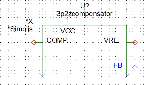
- Delete the power stage components until you have only the compensator symbols and wires
shown below:
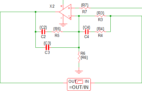
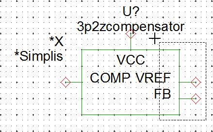
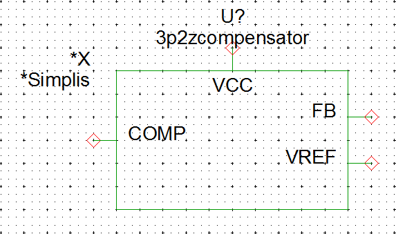
- Using either the keyboard shortcut H or the menu selection, , add module ports to the two inputs, the output, and the power supply of
the OpAmp as shown below. Note: As you place the module port symbols, you can press F5 to rotate the ports as needed.
- To save your schematic component to a file, select . Note: To keep your reusable blocks separate from the top-level schematics, it is good practice to save your schematics to a sub-directory of your schematic directory. This tutorial uses D:\SIMPLIS Tutorial for the schematic and a sub directory, D:\SIMPLIS Tutorial\Modeling Blocks, for the schematic components.
- Name your schematic component 3p2zcompensator.sxcmp. Note: The compensator schematic component file saved at this stage can be downloaded here: 3p2zcompensator_1.sxcmp.
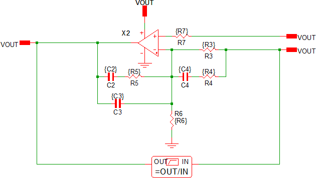
- After saving your work, double click each module port and change its name to those in
the table below:
Compensator Module Port Names
Port Function Port Name Reference Input (+ input) VREF Feedback Input (- input) FB Compensator Output COMP Power Supply Input VCC Result: When you finish renaming the module ports, the schematic should look like the following:
- Save your schematic component using Ctrl+S. The compensator schematic component file saved at this stage can be downloaded here: 3p2zcompensator_2.sxcmp.
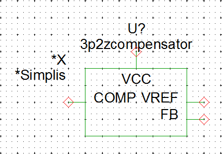
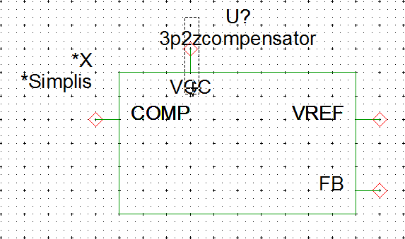
5.3.2 Create Symbol for Schematic Component
5.3.3 Enlarge the Symbol
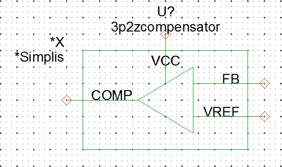
Although this symbol has all the needed electrical functionality, it could use some modification to make the function of the underlying block easier to see. In this next procedure, you will select the symbol pins and make the symbol larger than the auto-created size.
To enlarge the symbol, follow these steps:
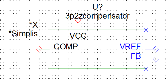
- Hold down the left mouse button and drag a box around the input pins on the right side
of the symbol. Make sure your box includes any portion of the VREF and FB text so these
elements will be selected.
 Result: The symbol pins, symbol pin text, and the vertical line on the right hand side are selected.
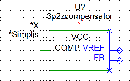
- Drag the selected portions of the symbol to the right 4 grid squares so your symbol
looks like the image below.
- Using the same technique as steps 1 and 2, select the FB pin, the FB pin
text and the horizontal line at the bottom of the symbol:
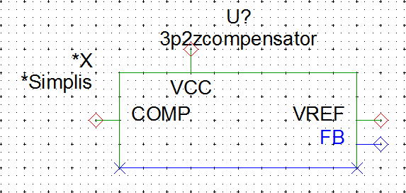
- Drag the selected portions of the symbol down two grid squares:
5.3.4 Move Symbol Pins
- To move the VCC pin, select the pin and text with a box as show below:
 Result: The VCC pin and VCC text are selected.
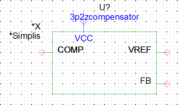 Note: The 3p2zcompensator text is also selected but this text is a symbol property and its position is controlled elsewhere. This symbol property is set to be centered on top of the symbol, so it does not matter that it is selected.
 - Move the selected VCC pin to the right two grid squares, bringing it to the
center of the symbol.
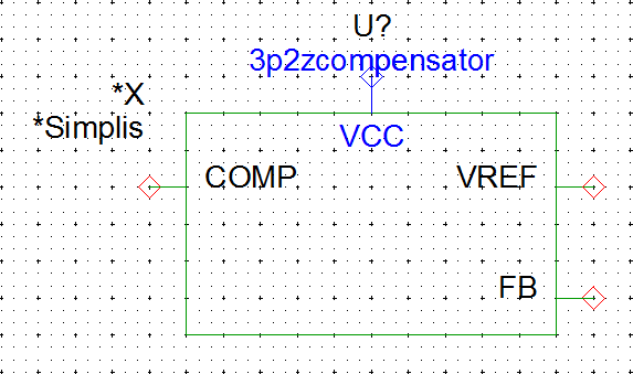
- Using the same technique as in steps 1 and 2, move the COMP, VREF and
FB pins as shown in the diagram below:Tip: It will be easier to move the VREF and FB pins if you move the VREF pin before you move the FB pin.
5.3.5 Add Graphical OpAmp Symbol
The final step in modifying the symbol is to add graphical lines which describe the functionality of the underlying symbol. Although this step is completely optional, these graphical elements are helpful for others to identify the function for each block on your schematic.
Drawing lines on symbols works just like drawing wires in the schematic editor. To add the lines, follow these basic guidelines:
- Double-click to start a line.
- Single-click to add a corner to a line.
- Right click or press Esc to end a line.
Using these techniques, draw graphical lines on the symbol so your symbol appears as follows:
5.3.6 Saving Symbols
As mentioned in the introduction to this section, symbols for schematic components are saved to the schematic component file along with the schematic. Other symbols for built-in parts, such as the resistor and waveform generator, are stored in symbol libraries. The program knows that this symbol, however, is configured to be saved to the schematic.
To save the symbol, follow these steps:
- Type Ctrl+S.
- Click Ok.
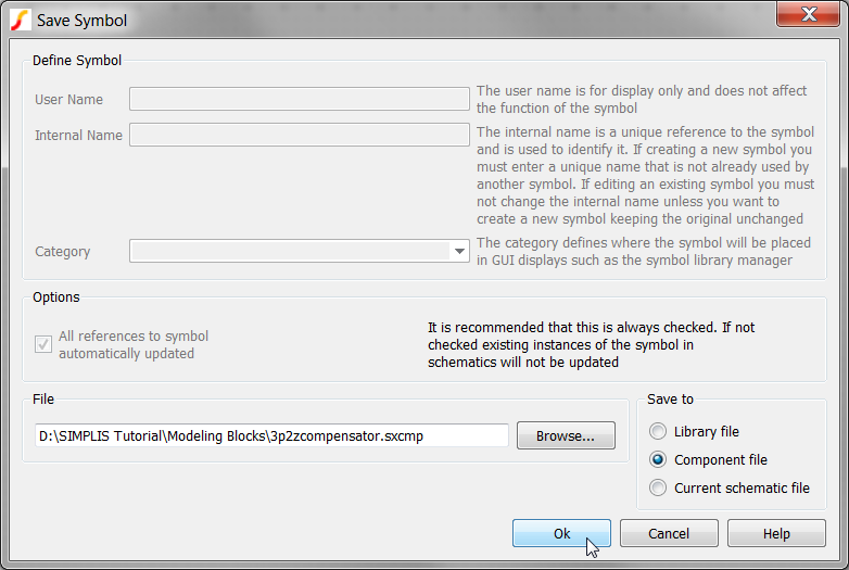
The compensator schematic component saved at this stage can be downloaded here: 3p2zcompensator.sxcmp.