Digital-Analog Interface Bridge
In this topic:
Netlist entry
Axxxx in out model_name
Connection details
| Name | Description | Flow | Type |
| in | Input | in | d |
| out | Output | inout | g |
Model format
.MODEL model_name dac_bridge parameters
Model parameters
| Name | Description | Type | Default | Limits |
| out_low | Analog output for 'ZERO' digital input | real | 0 | none |
| out_high | Analog output for 'ONE' digital input | real | 5 | none |
| g_resistive | Output conductance for 'RESISTIVE' digital input | real | 0.001 | none |
| g_pullup | Output conductance for 'STRONG' digital high input | real | 0.01 | none |
| g_pulldown | Output conductance for 'STRONG' digital low input | real | 0.01 | none |
| g_hiz | Output conductance for 'HI_IMPEDANCE' strength | real | 1.00E-09 | none |
| input_load | Capacitive input load (F) | real | 1pF | none |
| t_rise | Rise time 0 -> 1 | real | 1nS | ???MATH???1\text{e}^{-12} - \infty???MATH??? |
| t_fall | Fall time 1 -> 0 | real | 1nS | ???MATH???1\text{e}^{-12} - \infty???MATH??? |
| knee_high | Knee voltage logic high state | real | 3 | none |
| knee_low | Knee voltage logic low | real | 2 | none |
| sink_current | Input sink current | real | 0 | none |
| source_current | Input source current | real | 0 | none |
| v_smooth | Smoothing function offset voltage | real | 0 | ???MATH???0 - \infty???MATH??? |
| in_family | Input logic family | string | UNIV | none |
DC characteristics
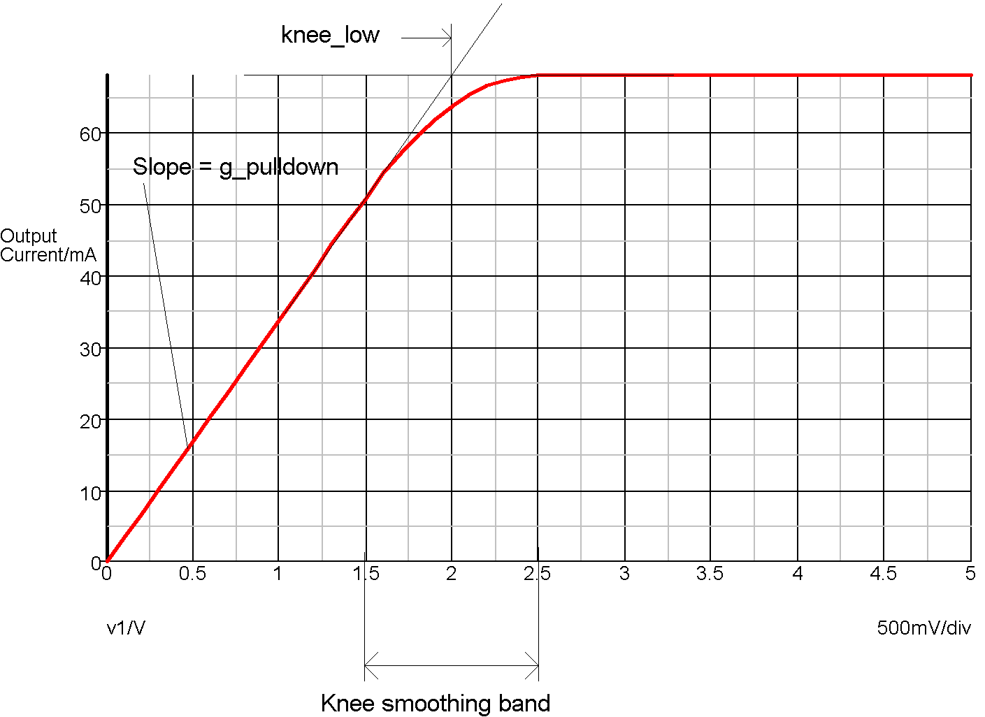
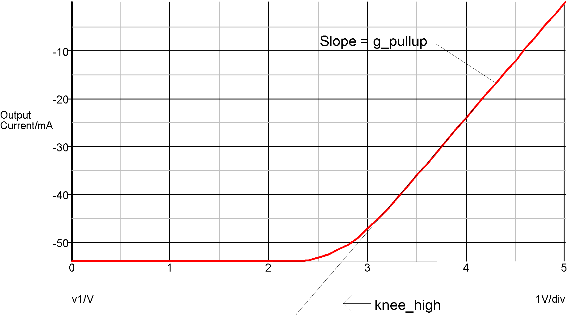
This digital to analog interface bridge is the main device used to connect digital signals to analog devices. The output provides an analog voltage and source resistance according to the state and strength of the driving digital input. The output has a non-linear characteristic that is a simplified model of a typical digital output stage. The following graphs show the output characteristics for the supplied high speed CMOS DA bridge. This has the following model parameters:
.model HC_dac dac_bridge
+ out_high=5         ; Logic high voltage
+ input_load=-31p    ; Compensates for added rise and fall time
+ t_rise=2n          ; Output rise time
+ t_fall=2n          ; Output fall time
+ g_pullup=0.024     ; 1/(logic high output resistance)
+ g_pulldown=0.034   ; 1/(logic low output resistance)
+ g_hiz=1e-9         ; 1/(high impedance output res)
+ knee_low = 2.0     ; voltage at resistive/constant current
+                    ; knee logic low
+ knee_high =2.75    ; voltage at resistive/constant current
+                    ; knee logic high
+ v_smooth = 0.5     ; Knee smoothing band
+ in_family="HC"

Logic '0' state - strength = STRONG
In the above graph, the slope of the curve at V=0 is determined by the G_PULLDOWN parameter. The 'knee smoothing band' is a transitional area where the output switches from a constant resistance to a constant current. The smoothing characteristic is a quadratic and is calculated to be smooth at all points. This is required for good convergence behaviour. The knee smoothing band starts at KNEE_LOW-V_SMOOTH and finishes at KNEE_LOW+V_SMOOTH.

Logic '1' state - strength = STRONG
If a state with RESISTIVE strength is applied to the input of a digital to analog interface bridge, the output has the characteristic of a pure resistor connected to the voltage associated with the input's state. In the example given above, this would be a 1k resistor connected to 0V for the logic '0' state and a 1k resistor connected to +5V for the logic '1' state. (1k is 1/G_RESISTIVE)
For the HI-IMPEDANCE strength, the output will look like a resistor of value 1/G_HIZ connected to a voltage half way between the two analog output states. (1G connected to 2.5V in the above example.)
When the input state is UNKNOWN the output will be as if it were half way between the two known states. This is a compromise solution. The UNKNOWN state does not have a parallel in the analog domain so instead it is treated as a transitional state. In some cases the UNKNOWN state occurs in transitional cases although this is not the correct meaning of UNKNOWN.
Switching Characteristics
When the logic state at the input changes, the output will transition from the current state to the target state in a time determined by T_RISE or T_FALL according to the direction of the state change.
| ◄ Digital-Analog Converter | Controlled Digital Oscillator ▶ |