Application B - Switching Losses and Measuring Efficiency
Based on the key concepts in topic 7.0, a new SIMPLIS Multi-Level MOSFET Driver was developed for version 8.0. This model has several improvements over the driver model developed in topic 7.0, but the core concepts have been preserved. In this topic, you will create a test bench for this Multi-Level MOSFET driver using an XY Probe that is new in version 8.0. Once you have characterized the behavior of this MOSFET driver, you will focus on how to use it to estimate the switching losses of the main power switch, as well as the overall efficiency, of a buck converter.
To download the examples for the Applications Module, click Applications_Examples.zip
In this topic:
Key Concepts
This topic addresses the following key concepts:
- In order to obtain accurate estimates of switching losses, a good driver model is equally as important as having a good MOSFET model.
- A simple test bench makes it easy to characterize a MOSFET driver. The test bench is helpful in understanding the interplay between the driver and the power MOSFET during switching transitions.
- When measuring power supply efficiency, good simulation technique is critical as
well as a good model.
- To obtain accurate results, the power supply system must be in a steady state.
- There is a strong correlation between the number of "forced" data points per switching cycle and the accuracy of efficiency and loss measurements.
What You Will Learn
In this topic, you will learn the following:
- How to use a simple test bench to characterize the output of a MOSFET driver .
- How different model levels of the Multi-Level MOSFET driver interact with Level 0 and Level 2 MOSFET models.
- How to use the efficiency calculator to estimate converter efficiency and the switching losses of power MOSFETs.
- Two critical simulation techniques necessary for obtaining accurate loss and efficiency estimates.
Background
The Multi-Level MOSFET driver was created to satisfy the driver model requirements discussed in topic 7.0. For convenience, those requirements are repeated here. The Multi-Level MOSFET driver allows you to do the following:
- Model the losses of a single MOSFET/driver combination including both conduction and switching losses.
- Parameterize the MOSFET driver model so that it may be used as a general purpose modeling block.
- Isolate the PWM driver input signal from the gate drive source and sink currents.
- Provide a parameterized asynchronous delay to the PWM input signal, allowing different values for the driver turn-ON delay and turn-OFF delay under no-load conditions.
In order to characterize the behavior of this driver, you will examine its operation under two different load conditions. To do this, you will create two test benches.
- First, a test bench that characterizes the Multi-Level MOSFET driver using a pure capacitive load..
- Second, a test bench that characterizes this driver while driving an N-channel MOSFET extracted to a level 0 model.
- Third, a test bench using a level 2 N-channel MOSFET.
Create Driver Test Benches
Since the ultimate objective is the evaluation of MOSFET switching losses with the Multi-Level MOSFET driver model, at least two test-bench circuits are needed. The first tests the driver model itself. To do this, we characterize Levels 0 and 1 of the Multi-Level MOSFET Driver using a pure capacitive load. The second is to test the Driver model while driving both Level 0 and Level 2 MOSFET models.
Test Bench #1
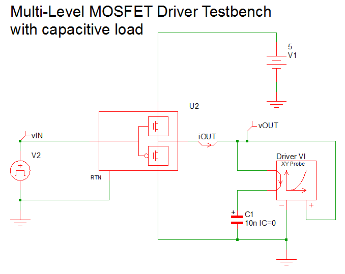
In the first test bench, you will test the driver modeling block with a pure capacitive load. To get started, open apps_b_1_multilevel_driver_test bench_cap_load.sxsch, which is shown below.
After opening the schematic, follow these steps to the model level parameters:
- Set the Level 0 parameters as shown below.
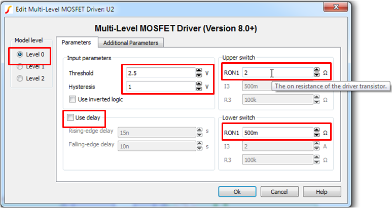 Note: the symbol is different depending on what model level is selected and whether or not the user is modeling delay. In this exercise, you will not use modeling delay.
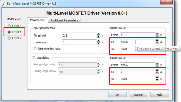
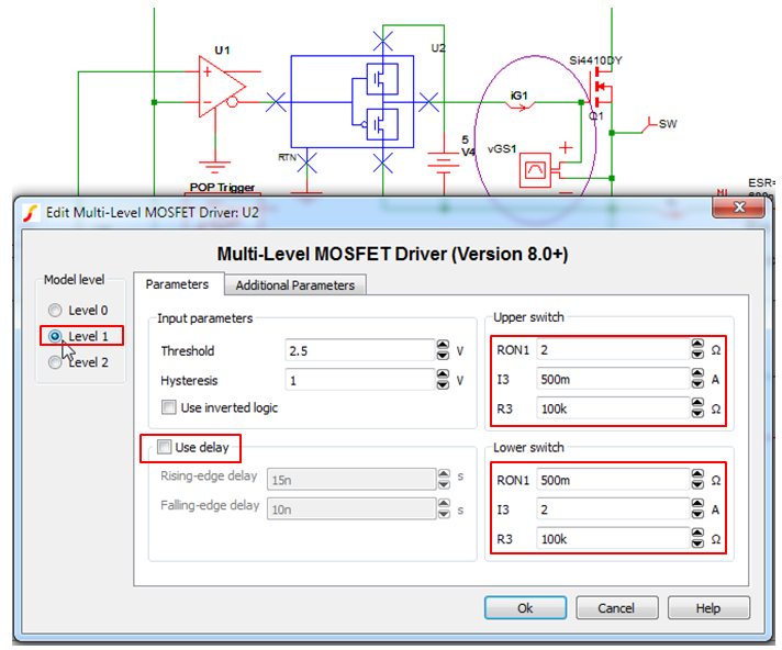
 - For Level 1, set the parameter values as shown below.
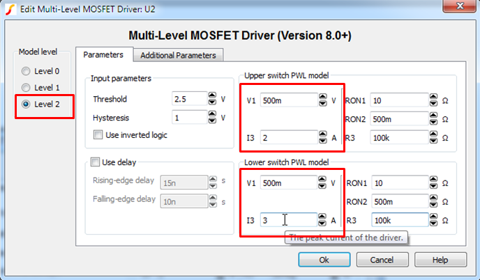
- Even though you will not explore the behavior of model level, for completeness,
set the following the parameter values for Level 2.
Model Level 0 Simulation
A detailed description of the Multi-Level MOSFET driver is
available by clicking on the Help button in the edit dialog for this part. The
Level 0 model is shown below.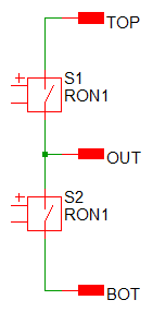
To run the Level 0 simulation, follow these steps:
- In the Model level section, select Level 0.
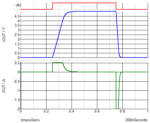
- Press F9.Result: After the simulation finishes, the graph window opens with the results noted below.
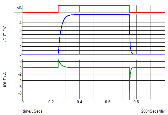
- When the capacitor voltage is initially rising, it is being charged by a current equal to the supply voltage across RON1 of the upper switch.
- The initial value of iOUT when the load capacitor is being charged is 5V / 2 Ohms = 2.5 A.
- The charging current iOUT then follows an exponential RC decay. As the capacitor becomes fully charged, iOUT approaches zero.
- The discharge current behaves in an analogous fashion with its peak current equal to -5V / 0.5 Ohms = -10 A.
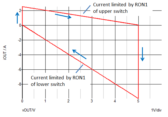
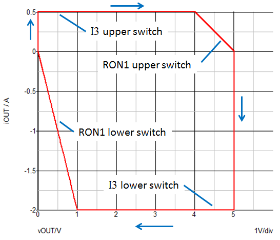
Viewing the iOUT and vOUT waveforms plotted in the iOUT vs. vOUT plane makes it easy to verify the key drive model break points from the graph below. You can also determine the values of RON1 for both the upper and lower switches from the slopes of the load lines during the charge and discharge intervals of the capacitor voltage vOUT.
Model Level 1 Simulation
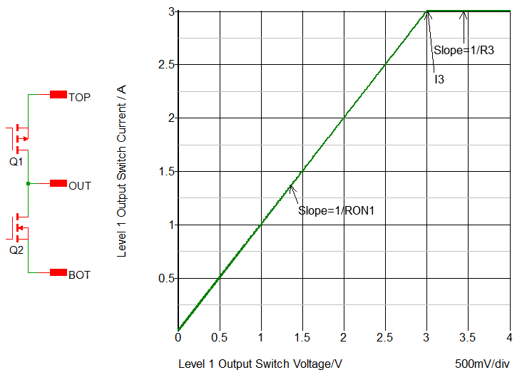
A detailed description of the Multi-Level MOSFET Driver is available by clicking on the Help button of the edit dialog for this part. The Level 1 model is shown below.
To run the level 1 simulation, follow these steps:
- In the Model level section, select Level 1.
- Press F9.Result: After the simulation finishes, the graph window opens with the results noted below.
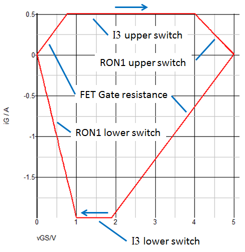
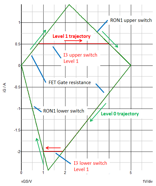
- With the Level 1 model of the Multi-Level MOSFET Driver, the maximum charging current is limited by I3 of the upper and lower switches Q1 and Q2.
- In this case the maximum charging current is 0.5 A and the maximum discharge current is -2 A.
From the iOUT vs. vOUT plot below, you can see that the load capacitor is charged with a constant current I3 by the upper switch until the voltage across the upper switch reaches a value of I3 * RON1, or (0.5 A * 2 Ohms) = 1 V. Beyond this point, the charging current follows an exponential decay determined by RON1 and the load capacitance. Similarly, during the discharge interval, the load capacitor is discharged by a constant current of I3 = -2 A of the lower switch until the voltage across the lower switch equals (2 A * 0.5 Ohms) = 1 V before beginning an exponential decay.
Test Bench #2
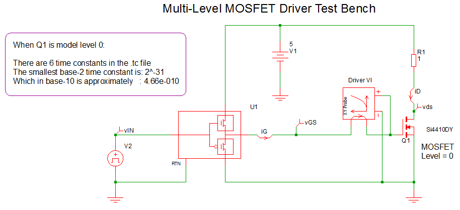
The next test bench looks at the performance of the combination of the Multi-Level MOSFET driver model and a Level 0 NMOS device driving a resistive load is shown below.
To launch this simulation, follow these steps:
- Open the 7.42_multilevel_driver_test bench_Lev0_mos_load.sxsch schematic.
- Verify that the Multi-Level MOSFET driver is set to Level 1.
- Verify that the Si4410DY MOSFET is set to Level 0.
- To run the simulation, press F9. Result: The steady-state waveforms generated by this schematic show the instantaneous switching as well as the same charging and discharging behavior of the gate capacitance that you observed in the test bench with the pure capacitive load. The only slight difference is that at the initiation of turn ON and turn OFF, there is an instantaneous step due to the 1.55 Ohm gate resistance of the Si4410DY MOSFET.
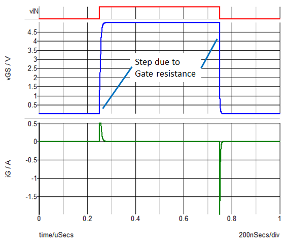
The effect of the MOSFET gate resistance is much more visible when you look at these same waveforms plotted in iG vs. vGS plane. During both the turn-ON and turn-OFF transitions, you see that the trajectory in the iG vs. vGS plane is dramatically altered by the gate resistance. Again, it is much easier to determine the critical modeling break points with this plot than it is with the time waveforms. In fact, even if you did not know the gate resistance initially, it is easy to measure gate resistance based on the slope of the trajectory in the iG vs. vGS plane.
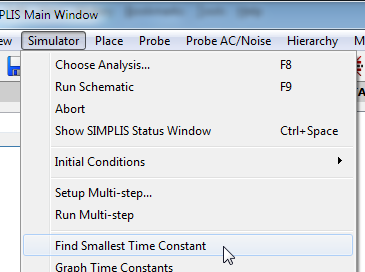
To find the smallest time constant, choose Simulator from the menu bar and then select Show Smallest Time Constant so that you can use this as a reference point in other test benches.
Test Bench #3
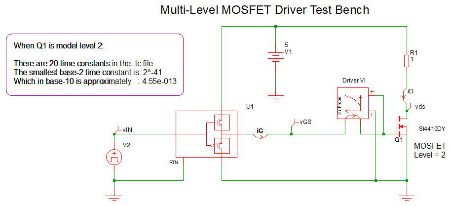
This test bench uses the same resistive load as before but the MOSFET model is a Level 2 instead of a Level 0 as shown below.
To run this simulation, follow these steps:
- Open 7.43_multilevel_driver_test bench_Lev2_mos_load.sxsch.
- Verify that the Multi-Level MOSFET driver block is set to Level = 1 and that the MOSFET Q1 is set to Level 2.
- Press F9.Result: The resulting waveforms show the expected Miller effect during turn ON and turn OFF. Note that the number of new topologies increases significantly when you go from a Level 0 MOSFET model to a Level 2. You also can see that the minimum time constant in base 10 is three orders of magnitude smaller with the Level 2 model.
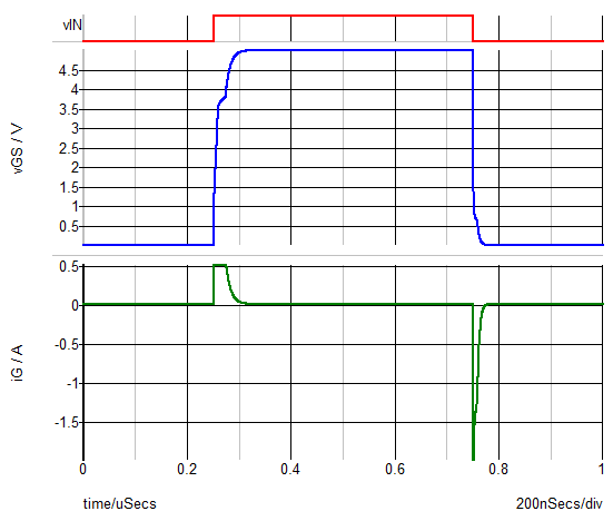
Although with the Level 2 MOSFET model, you can clearly see the Miller effect in the time waveforms of iG and vGS, the trajectory in the iG vs. vGS plane is exactly the same as with the Level 0 MOSFET model. Can you explain why this is so?

In order to obtain accurate estimates of switching losses, having a good driver model is equally as important as having a good MOSFET model. You need a simple test bench with a pure capacitive load to characterize the SIMPLIS Multi-Level MOSFET driver. This same approach can be used to characterize a hardware driver even if the published datasheet information is incomplete. Looking at the gate current and gate voltage waveforms in the iG vs. vGS plane reveals the critical break points needed to determine the appropriate Multi-Level driver model parameters.
Using the test benches presented in the topic, you can see how the current charging and discharging the gate of a power MOSFET is determined primarily by current limitations of the driver as well as by the gate resistance of the power FET. You can also can appreciate how a good test bench is helpful in understanding the interplay between the driver and the power MOSFET during switching transitions.
Before measuring switching losses and converter efficiency, follow these steps to perform a quick experiment.
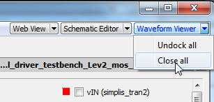
- Using the current test bench of 7.43_multilevel_driver_test
bench_Lev2_mos_load.sxsch, close any open waveform viewer results by
clicking Close all from the Waveform menu.
- Verify that the power MOSFET is set to Level 2.
- Verify that the driver is set to Level 1.
- To run the simulation, press F9.
- Without deleting any waveform results, change the driver level to level 0;
and then press F9 to run a second simulation.Result: In the time domain results, look at vGS and iG, during the turn-ON transition and you can see a noticeable difference in these waveforms. With the Level 0 settings, more current is available to charge the gate during the turn-ON transition. This should not be surprising given the parameter settings used for the Multi-Level MOSFET driver.
- Now look at the iG vs. vGS plot.
 Note: The signature of the Level 0 driver trajectory is different than that of the Level 1 driver trajectory in the iG vs. vGS plane. This way of picturing the circuit operation can be helpful in developing a fuller understanding of the complex behavior of a driver and MOSFET combination during the turn-ON and turn-OFF transitions of a power switch. This depth of understanding is important if you are to obtain accurate results when seeking to simulate switching losses and converter efficiency.
In the next two sections, you will examine the simulation techniques that are essential to obtaining accurate estimates of switching losses and power supply efficiency.
Simulate Switching Losses
A good vehicle to address the topic of simulating switching losses and converter efficiency is the buck converter developed in the SIMPLIS Tutorial (apps_b_6_SIMPLIS_tutorial_buck_converter.sxsch).
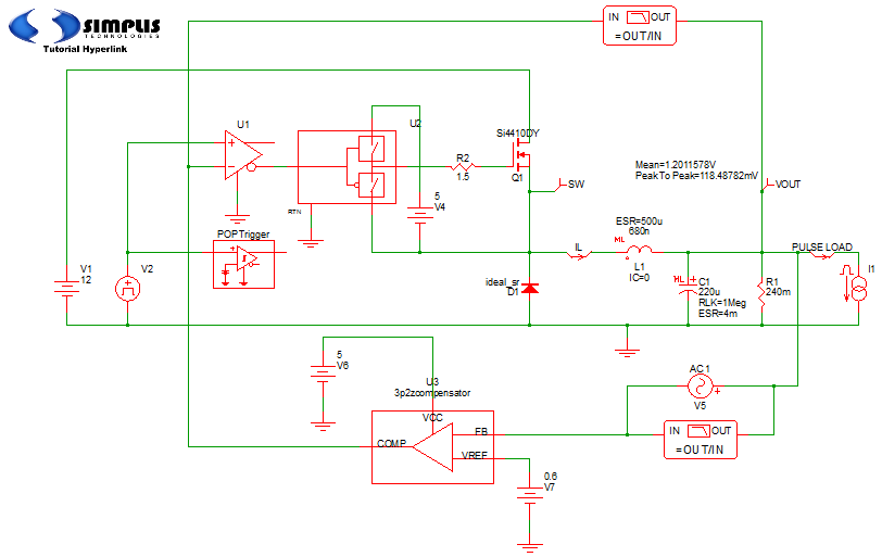
To modify this schematic in order to add appropriate probes for loss measurements and to improve the accuracy of the loss models of certain critical components, follow these steps.
- Add probes to measure the gate current iG and the gate-to-source voltage vGS as
shown in the highlighted oval near Q1 in the figure below. Result: When you do this, you eliminate the resistor R2 that was in series with the gate pin of Q1 in the original Tutorial schematic
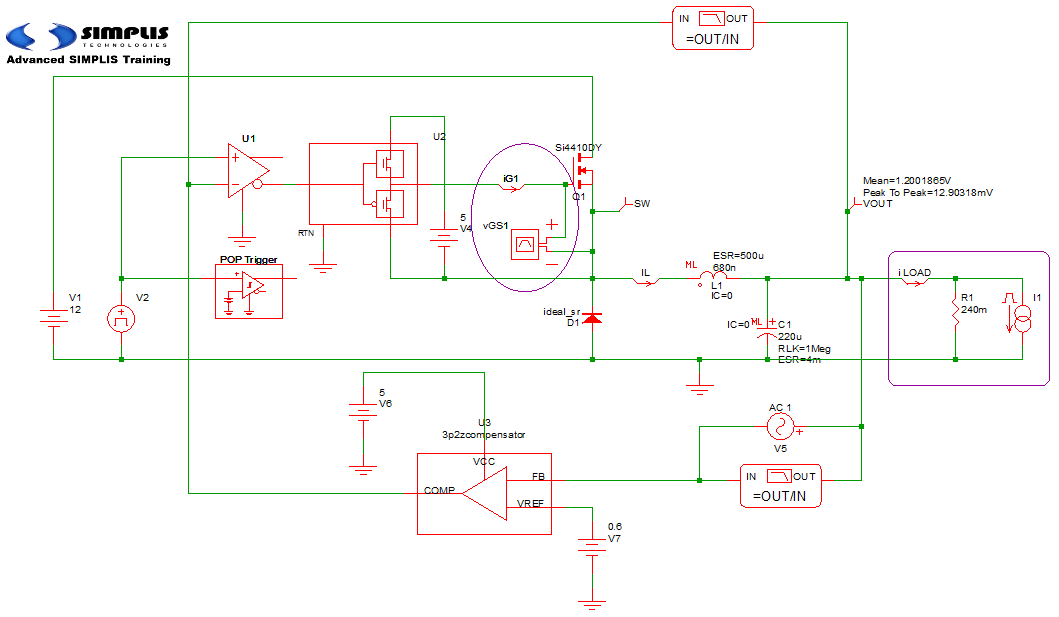
- To make it easier to measure the total load current, rearrange the relative positions of the in-line current probe iLOAD and the load resistor R1 and load current source I1 as indicated in the highlighted rectangle at the far right in the illustration above.
- Make sure that the power MOSFET Q1 is set to Level 2.Note: In order to accurately model switching losses, it is essential to use a model level that accurately simulates the switching transitions.
- Verify that the other MOSFET parameters are set to the values shown here.
- To make sure the driver model can accurately simulate the driver transitions, verify
that the driver is set to Level 1 and that the other parameters agree with those
shown below.
 Note: The schematic resulting from this changes is apps_b_7_SIMPLIS_tutorial_buck_converter_mods.sxsch
Time Domain Waveforms
In this section you will verify that the time domain waveforms do, in fact, model the switching transitions of the power switch Q1.
As will become clear in this discussion, accurate loss and efficiency measurements require that the converter system be in steady state. You will also see that it takes a surprising number of data points per switching cycle to obtain sufficient resolution of the high frequency switching waveforms to yield accurate loss measurements. In all of the following simulations, you will simulate exactly one cycle of steady state operation. This allows you then to get the maximum benefit of each data point that is calculated and output from a simulation.
For the next simulation, follow these steps:
- Open the schematic, apps_b_7_SIMPLIS_tutorial_buck_converter_mods.sxsch.
- From the menu bar, select , and then go to the Periodic Operating Point (POP) tab.
- Click the Advanced... button.
- Verify that the Number of cycles output is set to 1.
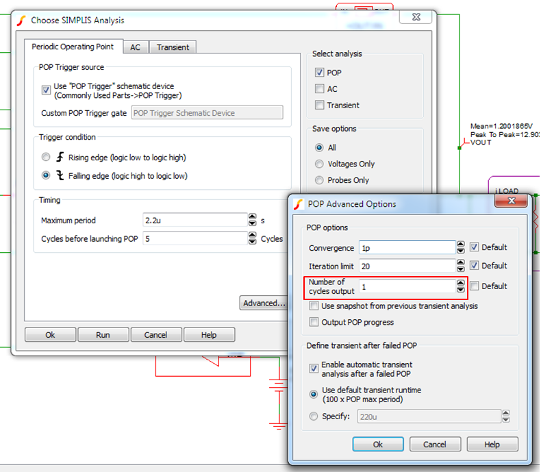
- Go to the Transient tab and set the Number of plot points to
5k.
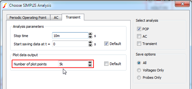 Result: This combination of POP and Transient analysis settings will result in the simulation of one steady-state conversion cycle and SIMPLIS will output a minimum of 5000 equally spaced data points.Note: When the simulation objective is to measure various closed-loop performance attributes of a switching power supply, such as a step-load transient, the required number of data points per cycle is modest. Indeed, 5000 data points per conversion cycle would be excessive in the extreme. However, when trying to measure switching losses that occur during the turn-ON and turn-OFF transitions of the power switch, as shown below, using 5000 data points per switching cycle will typically reduce the numerical sampling error of a switching device loss measurement to less than 0.5%.
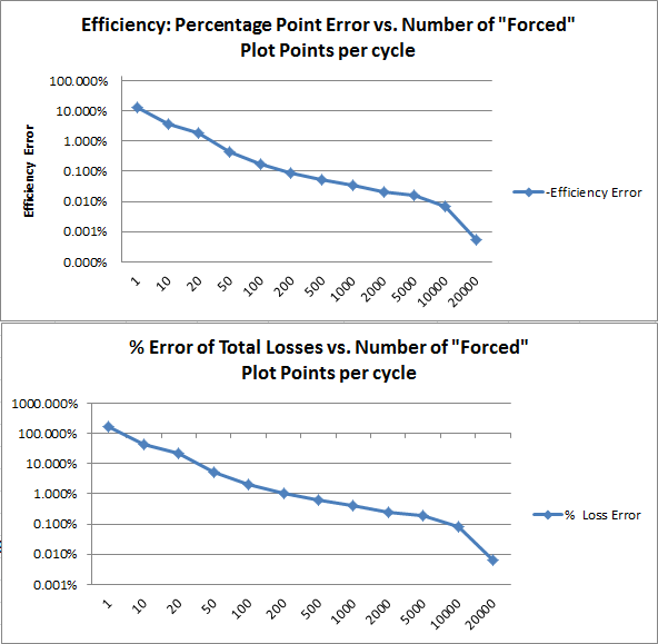
- Run a POP analysis of this circuit. Result: Below are the resulting steady-state waveforms of the gate voltage vGS1, gate current iG1, switch node voltage SW and the inductor current iL.
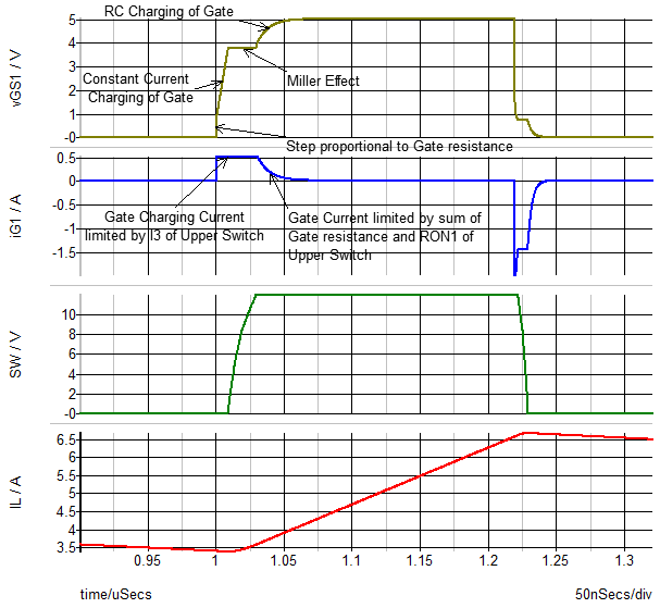
Observe the following results:
- During the turn ON transition, the gate current steps up to a value of I3 of the upper switch in the Multi-Level driver model causing a small step in the gate voltage that corresponds to the resulting voltage across the gate resistance of Q1, which in this example is 1.55 Ohms.
- the gate voltage reflects the fact that the input capacitance of Q1 is charged by a constant gate current equal to I3 until the gate voltage reaches a value that allows all the inductor current iL to flow through Q1. At this point, the drain-to-source voltage of Q1 begins its transition from high to low and the switch node SW transitions from low to high.
- During the turn ON switching transition, assuming the gain of Q1 is reasonably high, the gate voltage plateaus at a voltage such that the rate of change of drain-to-gate voltage is equal to gate charging current divided by the nonlinear gate-to-drain capacitance.
- Once the turn-ON switching transition is complete, then the gate voltage continues to be charged up to its maximum value. This rate of charge is set by I3 until the voltage difference between the driver positive supply node and the gate capacitor decreases to the point where the charging current is then limited by the voltage drop across RON1 of the upper switch + the gate resistance.
- The gate discharge and the resulting turn OFF transition happen in an analogous
fashion as shown below.
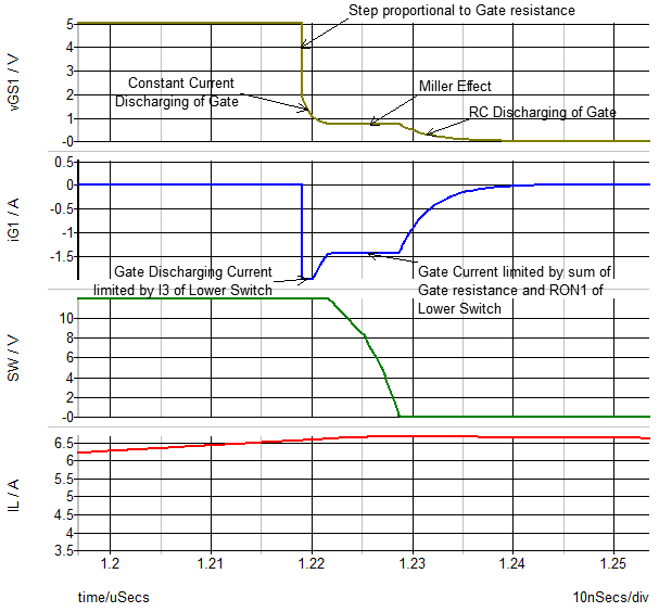
- There is one possible difference in the discharge waveforms. In this example, you can see a second plateau in the gate current waveform iG1 during turn OFF that was not present during the turn ON transition. This occurs because by the time that the gate voltage reaches the voltage corresponding to the maximum inductor current iL, the terminal voltage vGS is low enough that the discharging current is limited by the series combination of gate resistance + RON1 of the lower switch in the driver model.
Measure Power Supply Efficiency
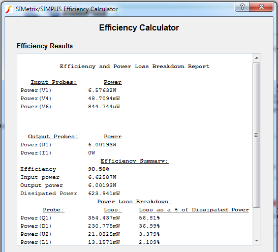
The final step in this topic is to demonstrate how to measure the efficiency of a switching power supply, especially the losses associated with the power switch Q1. The final schematic apps_b_8_SIMPLIS_buck_converter_measure_losses.sxsch shows the result of employing the Efficiency Calculator to conveniently summarize all the critical losses in the test bench circuit.
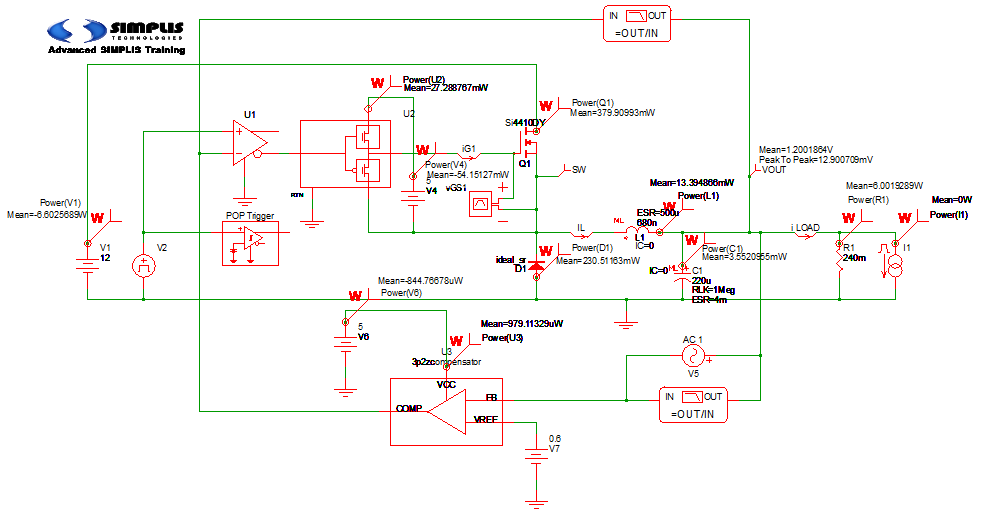
After adding the power probes to the schematic and defining the input sources and output loads, a steady-state POP simulation is run. A Periodic Operating Point analysis always results in steady-state time-domain waveforms that are an exact integral number of steady-state switching cycles. This makes measuring the average powers dissipated very straightforward.
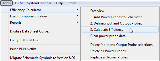
To run the efficiciency calculation, select from the menu bar.
The results of the Efficiency Calculator are shown below. These results are calculated based on the average power dissipated by each component with a power probe attached to it. As is often the case, the largest contributor to the total losses is the power lost in the main power switch Q1. Second is the loss in the rectifying diode D1.
Discussion
The above discussion focuses on average losses over a complete steady-state switching cycle. When optimizing the combined design of a driver and a MOSFET, you need to look at the component portions of the switch losses, turn ON, turn OFF and conduction losses. There are a number of ways to do this. But one very easy one is shown here.
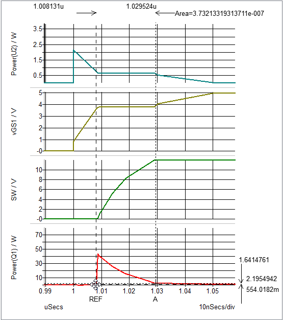
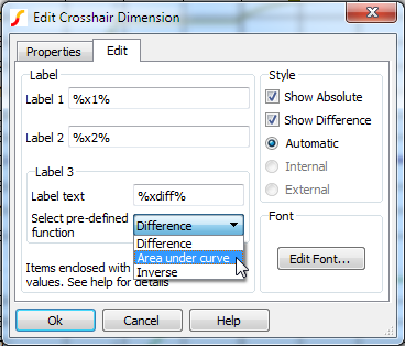
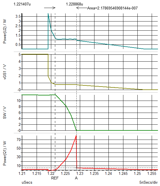
Notice that the calculated the area is under the instantaneous power dissipation curve for Q1 during the turn ON transition. To accomplish this, set the cursors at the beginning and the end of the turn ON transition, and then double click on the time difference display. This action opens up a dialog window that allows us to request the display of the area under the selected curve between the REF and A cursors.

The result is that you have now calculated the energy dissipated in the MOSFET during each turn ON transition. In this case, 0.37 uJ at 500 kHz results in a loss of 0.185 W.
Using the same approach to measure the turn OFF losses, you obtain 0.22uJ of turn OFF energy, which results in a loss of 0.109 W. Using this approach, you designer can scale the loss results by the switching frequency, which can be very convenient when trying to optimize the overall design.
As is clear from the waveforms above, you would use the same approach to examine the losses in the driver circuit.
This modeling approach provides a powerful method for optimizing the design of a driver - power switch combination. The parameterization of the driver allows you to independently control the turn ON and turn OFF driver characteristics. The analysis approach allows you to optimize the driver characteristics and the power MOSFET selection according to the application requirements.
- First, the steady-state circuit solution is extremely accurate and is obtained very quickly. Typically, POP runs much faster that a long transient. The POP output is an integral number of cycles. This means that in order to find the average power dissipation over an integral number of switching cycles, you can average the instantaneous power dissipation waveform. There is no need to carefully arrange cursors to average correctly.
- The other thing that POP accomplishes is that you dd not need to determine how
long a transient needs to be run in order to approach a reasonable steady-state
solution. Below is a plot of both the per-cycle converter efficiency and the
per-cycle efficiency error during a long transient simulation.
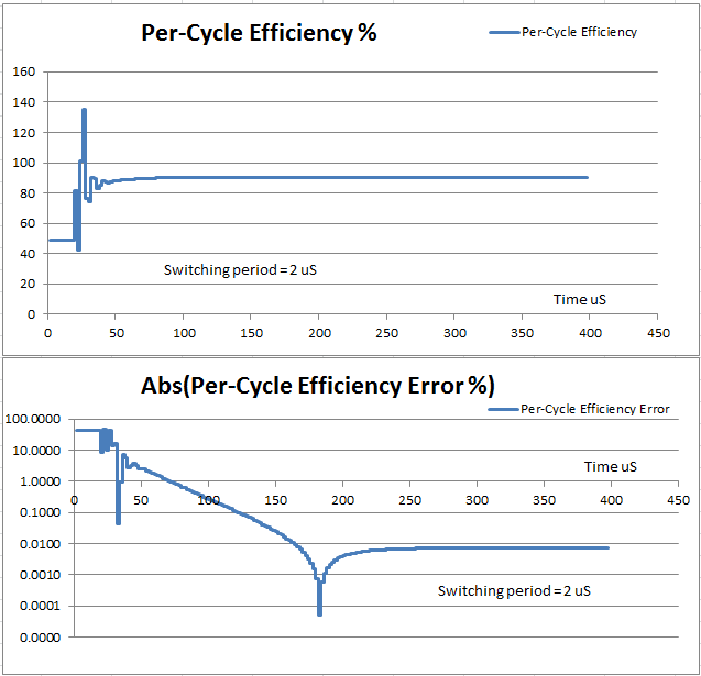 Since the switching period is 2 uS, this plots the efficiency for about
200 conversion cycles. This example circuit is not complex and is well designed
and well compensated; therefore, in this case and for this set of initial
conditions, you need to wait for only about 50 conversion cycles for the
efficiency error to be less than 0.1 percentage points. However, for more complex
circuits or worse initial conditions, the wait could be much longer. Also, extreme
care must be taken when running simulations that require so many data points. The
one simulation required to create these plots took up more than 10% of a laptop
hard drive.
Since the switching period is 2 uS, this plots the efficiency for about
200 conversion cycles. This example circuit is not complex and is well designed
and well compensated; therefore, in this case and for this set of initial
conditions, you need to wait for only about 50 conversion cycles for the
efficiency error to be less than 0.1 percentage points. However, for more complex
circuits or worse initial conditions, the wait could be much longer. Also, extreme
care must be taken when running simulations that require so many data points. The
one simulation required to create these plots took up more than 10% of a laptop
hard drive.
An example showing how to plot out per-cycle efficiency and losses may be found in the F11 window of the schematic apps_b_9_measure_per_cycle_losses_and_efficiency.sxsch.
Conclusions and Key Points to Remember
- When using simulation to estimate switching losses in a switching power supply, a good driver model is as important as having a good MOSFET model. For accurate results, it is essential to model the current limitations of the driver.
- A simple test bench makes it easy to characterize a MOSFET driver. The test bench is also helpful in understanding the interplay between the driver and the power MOSFET during switching transitions.
- When measuring power supply efficiency, in addition to good models, good
simulation technique is critical.
- To obtain accurate results, the power supply system must be in a steady state. As the system model becomes more complex, it becomes more and more time consuming to use a long simulation to reach steady state. Determining how long a transient is required to achieve a desired level of accuracy is arduous and will help you appreciate the real power of the POP analysis.
- There is a strong correlation between the number of "forced" data points per switching cycle and the accuracy of efficiency and loss measurements. By using only one thousand data points per cycle in this example, you were introducing a data sampling error of about 0.4 percentage points of efficiency. In other words, this data sampling error, in a 90% efficient dc-dc converter was equivalent to 4% of the total losses in the system. To reduce the sampling error below 1% of the total losses (or 0.1 percentage points), you would have needed to use 10,000 data points per cycle.
- Long transients and thousands of data points per switching cycle are a dangerous combination. It takes very little effort to fill up your hard drive. Using the Periodic Operating Point analysis and outputting only one cycle of data dramatically reduces this possibility.