Using Schematic Editor for CMOS IC Design
In this topic:
MOSFET Symbols
Four MOSFET symbols are supplied for use in CMOS IC design. These are:
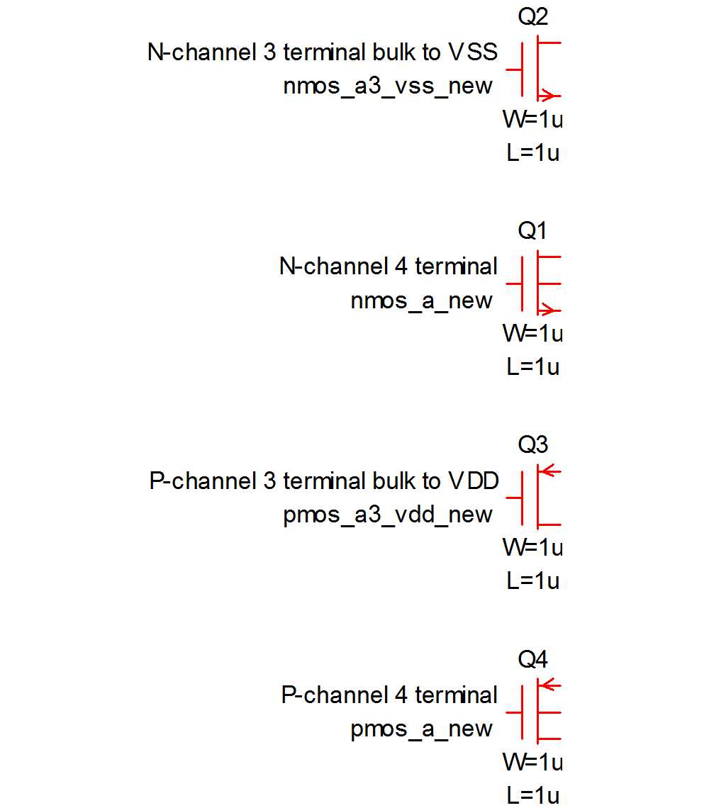
These symbols have the model name N1 for the N-channel types and P1 for the P-channel types. These names can of course be changed after being placed on the schematic, but this would be time consuming to have to do each time. To avoid having to do this, you can do one of the following:
- Modify your SPICE model files so the devices are always called N1 and P1
- Modify the standard symbol so the model name corresponds to your SPICE models.
- Create a new set of symbols for each process you use.
- Select menu . This will open the startup script in a text editor window. The startup script is automatically run each time the program starts.
-
Enter a DefButton command for each toolbar button you wish to redefine. For the MOS symbols the commands will be one or more combinations of the following:
- DefButton NMOS4 "inst /ne your_nmos4_symbol"
- DefButton PMOS4 "inst /ne your_pmos4_symbol"
- DefButton NMOS3IC "inst /ne your_nmos3_symbol"
- DefButton PMOS3IC "inst /ne your_pmos3_symbol"
Edit Length and Width
A popup menu Edit MOS Length/Width... will edit L and W properties. The menu is initially hidden but can be enabled by setting the option variable EnableLWEditMenu. You can do this by typing this command at the command line:
Set EnableLWEditMenu
You will need to restart SIMetrix to bring this into effect.
Automatic Area and Perimeter Calculation
The optional popup menu Edit MOS Length/Width... (See Edit Length and Width) edit device length, width and scale factor. These menus alter the symbol properties W, L and M for width, length and multiplier.
The symbols described above have been designed in a manner such that additional parameters such as AS, AD, PS, PD, NRS and NRD may be automatically calculated from width and length. To use this facility append the value property with the parameter definitions defined as expressions. E.g.:
N1 AD={2*%W%+0.8u}
The above device will have an AD parameter calculated from "2*width+0.8u". Note that the formula is enclosed in curly braces ('{', '}') and width and length expressed as %W% and %L% respectively. You can use similar expressions for any other parameter.
As an alternative, you can define AS, AD etc. as a parameter expression in a sub-circuit. See Subcircuits for more details.
Editing the MOS Symbols
You may wish to create your own MOS symbols for each process you use. We suggest that you always make a copy of the standard symbols and save them with a new name in your own symbol library.
Once you have your copied version, you can edit it to suit your IC process. In most applications, you will probably only need to edit the VALUE property. See next paragraph.
Editing VALUE property
The VALUE property defines the model name and all the device's parameters except length, width and the multiplier M. The standard VALUE property defines just the model name and this defaults to N1 for NMOS devices and P1 for PMOS devices. You should edit these to match the model name used in your process.
In addition (as described in Automatic Area and Perimeter Calculation) you can append the VALUE property with other parameters such as AD, AS etc. and define these as expressions relating width (using %W%) or/and length (using %L%.)
To Edit the Default Values of L and W
Edit the L and W properties as appropriate.
To Edit the Hidden Node for 3 Terminal Devices
The hidden bulk node for three terminal devices is defined by the BULKNODE property. This defaults to VSS for NMOS devices and VDD for PMOS devices.
| ◄ Load Component Values | Further Information ▶ |