SystemDesigner Tutorial
This tutorial explains the following:
- How to set up the schematic file for a new design
- How to place components on the schematic
- How to edit parameter values on the components
- How to run the SystemDesigner simulations
In this topic:
Starting a New Design
To start a new design, follow these steps.
- From the Schematic Editor menu bar, select File | New.
- From the menu bar, select File | Save and type a file name in the Save As... window. This tutorial uses myExample as the file name.
- From the Schematic Editor menu bar, select SystemDesigner | Edit SystemDesigner Clocks....
- At the prompt to load the default properties, click Yes
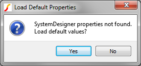 Result: After you click Yes, the default properties are written to the schematic file, and then the Edit SystemDesigner Clocks dialog appears.
 - Set the SysClk label and frequency as shown below.
The default settings in the other columns are valid.Column Value Label 2Meg Frequency (Hz) 2Meg 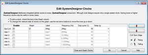
- To save your clock information, click OK.
or
To view a simulation of the clocks, click Close and Graph Clocks.Result: A simulation including only the global clocks executes, and two cycles of the lowest clock frequency appear on the graph viewer.
For more information about setting up clocks, see SystemDesigner Clocks.
Adding Components to the Schematic
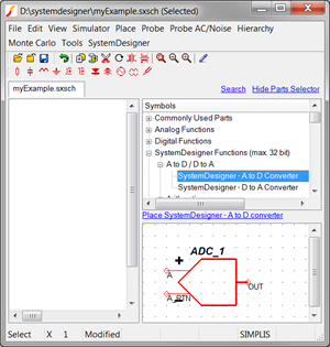
You can use the Parts Selector on the right side of the Schematic editor to place allSystemDesigner components. If the Parts Selector pane is hidden, click the blue Show Parts Selector link in the upper-right corner of the schematic.
All SystemDesigner components are in the SystemDesigner Functions (max. 32 bit) section of the selection tree as shown below:
You have a choice of ways to select components to place on the schematic:
- Double click a part in the selection tree.
or
- With a part selected in the Parts Selector, click the hyperlink between the
selection tree and the symbol preview.
or
- To place multiple instances of the same component, right click on a part in the selection tree and select the second item in the drop-down menu: <part name> (repeat).
After you select a part, move your cursor onto the schematic and then click where you want to place that component.
To place parts for this tutorial example, follow these steps.
- From the A to D / D to A section of the SystemDesigner Functions (max. 32 bit), select and place SystemDesigner - A to D Converter.
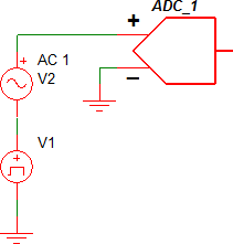
- To place a waveform generator, type the keyboard shortcut, W with your cursor on the schematic, and then click to place the component.
- From the Commonly Used Parts section of the Parts Selector:
- Select and add AC Source (for AC Analysis).
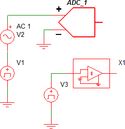
- Select and add Ground.Result: At this stage, the schematic should have three components and a ground symbol.
- Wire the waveform generator, AC source, and ground to the ADC as shown below with
the green lines.
- To enable simulation of the design with the SIMPLIS POP and AC analyses, follow
these steps to place a POP trigger and a square wave source that drives the POP
trigger device.
- To place another waveform generator, type the keyboard shortcut W with your cursor on the schematic, and then click to place the component.
- To place the POP Trigger device, click the Search link at the top of the Parts Selector and type POP in the search box; then click OK and click on the schematic to place the Pop Trigger.
- Wire the Waveform generator V3 to the POP trigger device and add a ground
symbol from the Commonly Used Parts section of the Parts Selector.Result: The schematic should now look like this:
- To place the special probes, follow these steps using the Probes category in
the
SystemDesigner Functions (Max 32 bits) section of the Parts Selector.
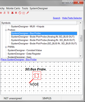
- Select and place a SystemDesigner - Bus Probe and a SystemDesigner - Bode Plot Probe (Analog IN, SD_BUS OUT).
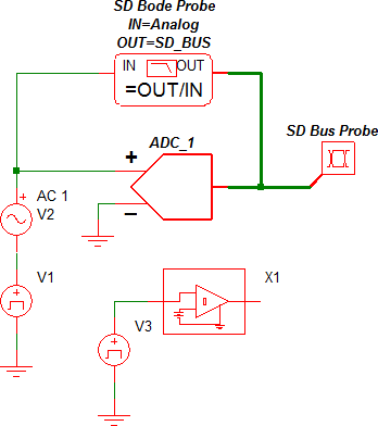
- Wire these probes as shown below with a SystemDesigner bus connected to the OUT pin on the Bode Plot Probe.
- To save the schematic at this point, select File | Save.
In the next section, you edit parameter values for four of the components and set up the analysis types.
Editing Component Values
If you are not sure about the purpose of a parameter as you edit the components, hover your mouse cursor over the parameter name or over the related text box or menu to view the associated tool tip.
To edit components for this tutorial example, follow these steps:
- Double click on the ADC symbol on the schematic to bring up the edit dialog.
- Set the LSB weight to 200mas shown below:
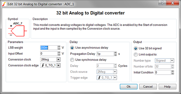 Note: The dialog box for each device that uses clocks is populated with values set in the SystemDesigner Clocks dialog. The default clock is the system clock (SysCLK) and is selected for this ADC. In the first procedure in this tutorial, you set the Label of the SysCLK to 2Meg which now appears in the Conversion Clock field and, in this tutorial, is appropriate for the design.
 - Click Ok to close the edit dialog.
- Double click the waveform generator V3, and make the following changes:
When you change the Pulse value, the offset and Amplitude change automatically as shown below.Parameter Value Frequency 1Meg Pulse 5 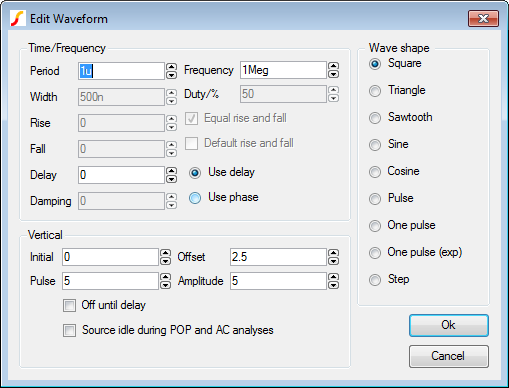
- Double click the V1 waveform generator and change these parameter values:
Parameter Value Initial (voltage) -1 Wave shape Sine Source idle during POP and AC Analyses Check 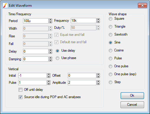
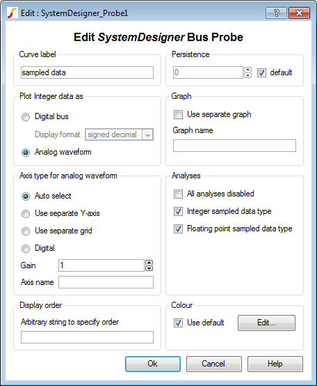
- Double click the SystemDesigner bus probe:
- In the Curve label text box, type sampled data.
- In the "Plot Integer data as" section, select Analog waveformas shown below.
To set up the analysis types and set the analysis parameters, follow these steps:
- From the menu bar, choose Simulator | Choose Analysis, and check all three analyses: POP, AC, and Transient.
- Set the parameters as listed below.
POP AC Transient Select Use "POP Trigger" schematic device. Stop Frequency = 10Meg Stop time = 100u Maximum Period = 1.1u - Click Ok, and then, to save your schematic, select File | Save. A completed schematic example can be downloaded here: myExample.sxsch.
Running SystemDesigner
SIMPLIS SystemDesigner has two sampled-time simulation modes: signed integer and double-precision
floating point. The default sampled data type is Signed Integer. The
current default is labeled in the SystemDesigner menu with => as shown below: 
The following table lists the menu options to set a default simulation type from the SystemDesigner menu.
| Mode | To set default simulation |
| Signed integer | SystemDesigner | Set Default (F9) Sampled Data Type | Signed Integer |
| Double-precision floating point | SystemDesigner | Set Default (F9) Sampled Data Type | Double Precision Floating Point |
To run the default simulation, which, in this case, is the signed integer simulation, do one of the following:
- Select the Simulator | Choose Analysis... menu, and then click Run.
- Type F9.
- Run the simulation from the SystemDesigner menu: SystemDesigner | Run w/ Sampled Data Type | Signed Integer.
Signed-integer simulation results:
- After you run a simulation in signed integer data mode, the SIMetrix/SIMPLIS command
shell shows the following message:
Running with Signed Integer Data Type
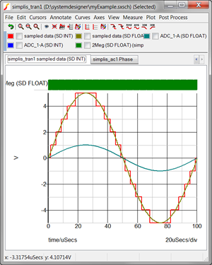
- The graph window appears with the curves for the selected data type as shown in the
example below:
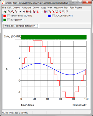
- In the graph above, the curves are represented as follows:
- The Blue curve is the analog input voltage, which is a pure sine wave with an amplitude of 1V and a frequency of 10kHz.
- The Red curve is the time-sampled analog input voltage, which has been quantized in voltage level.
- The Green curve is the 2 MHz sampling clock.Note: In Step 2 of Editing_Component_Values, you set the LSB weight of the ADC to 200mV. Since the input waveform has a maximum amplitude of 1V, the maximum value of the time-sampled output is +/-1V/200mV =+/- 5 LSBs.
Because the LSB weight of the ADC is large, not every sampling clock creates a change in the ADC output; therefore, the sampling clock has a higher frequency than the time-sampled output waveform.
To run the double-precision floating-point simulation, select SystemDesigner | Run w/ Sampled Data Type | Double Precision Floating Pointfrom the menu bar.
Double-precision floating-point simulation results:
- The SIMetrix/SIMPLIS command shell now has an additional message:
Running SystemDesigner with Double Precision Floating Point Data Type
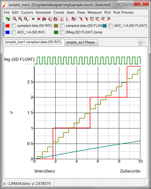
- The graph output has the results of the double-precision floating-point simulation
overlaid on the integer data results:
- In addition to three curves from the integer-sampled data-type simulation, the graph now has the time-sampled data for the double-precision floating-point simulation.
- The olive curve shows the input voltage that is converted on every 2 MHz clock edge.
- The vertical amplitude is NOT quantized into 200mV levels.
- Zooming into the waveform from 0 to 10us shows the waveform detail:
- During the double-precision floating-point data-type simulation, SIMPLIS runs all
three analyses:
- The POP analysis runs first.
- After a successful POP analysis completes, the AC analysis runs.
- The last analysis is the transient analysis which has the waveform data.
AC analysis results
To see the AC analysis results, click on the simplis_ac1 Phase tab:
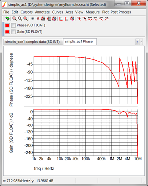
- The SystemDesigner Bode Plot Probe is connected to probe the gain and phase of the transfer function of the ADC.
- The theoretical transfer function is a gain with a zero-order sample and hold at the sampling clock frequency of 2MHz.
- The low frequency gain should be 1/(LSB Weight) = 5 = 13.98dB.
- The zero order sample and hold produces a phase wrap at the sampling frequency and at every harmonic higher than the sampling frequency as expected.