5.4 Using Schematic Components
This section focuses on placing hierarchical components and navigating between schematic levels.
In this topic:
Key Concepts
The following key concepts are addressed in this section:
- Schematic components can be placed with either the full path or with a path relative to the parent schematic.
- Schematic designs using relative path symbols are portable and can be easily shared with colleagues.
- The keyboard shortcut Ctrl+E allows you to descent into child components; Ctrl+U takes you back up to the parent level.
What You Will Learn
In this section of the tutorial, you will learn the following:
- How to place the symbols contained in schematic component files.
- How to navigate between hierarchical schematics.
5.4.1 Placing Schematic Components
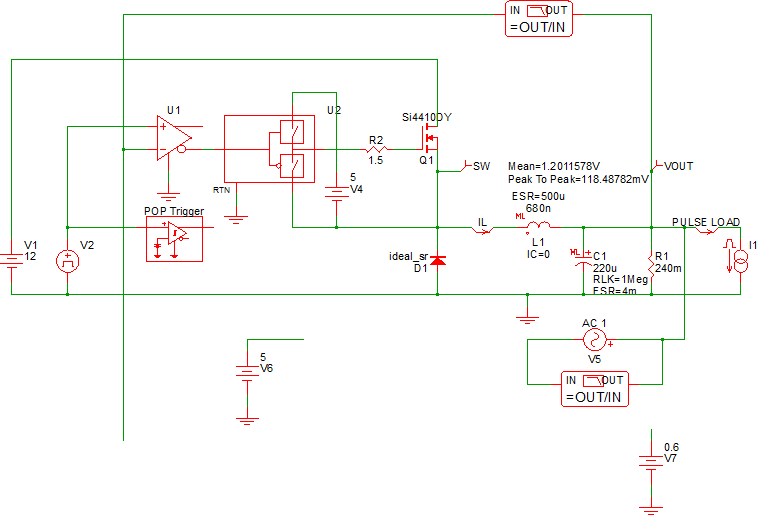
In this section you will start with the schematic from the end of section 5.2 Set up a Load Transient Simulation and place the schematic component symbol created in 5.3 Creating Hierarchical Schematics.
Open the schematic you saved at the end of section 5.2 Set up a Load Transient Simulation or use 12_SIMPLIS_tutorial_buck_converter.sxsch from simplis_tutorial_examples.zip.
To place the compensator hierarchical schematic symbol, follow these steps:
- Delete the compensator symbols you moved into the 3p2zcompensator hierarchical block in
section 5.3 Creating Hierarchical Schematics. Result: Your schematic should look similar to this:
- From the menu bar, select .Result: A File Selection dialog opens.
- Open the Modeling Blocks folder.
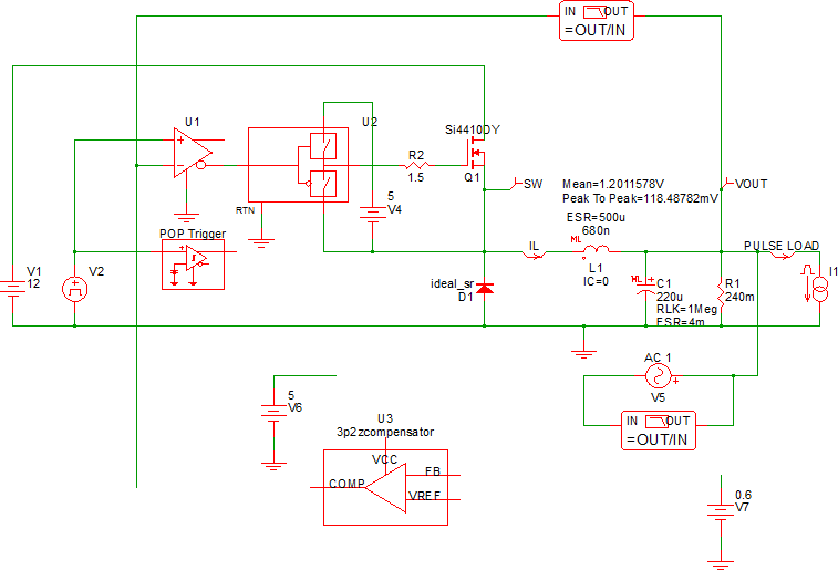
- Select the 3p2zcompensator.sxcmp schematic component, and click Open.
- Place the symbol where the compensator components used to be:
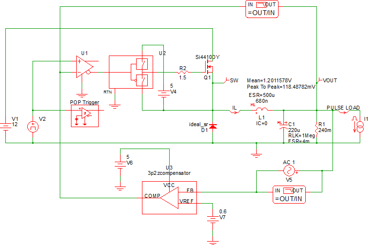
- Wire the compensator to the power stage. You can move symbols around to clean up the
wiring. After this step, your schematic should look like the following:
5.4.2 Save your Schematic
To save your schematic, follow these steps:
- Select .
- Navigate to your working directory where you are saving your schematics.
- Name the file 13_my_buck_converter.sxsch.Note: A schematic saved at this state can be downloaded here: 13_SIMPLIS_tutorial_buck_converter.sxsch.
5.4.3 Cleanup Top Level F11 Window
When you save a schematic to a new name or save a schematic to a schematic component, the content of the F11 window is also copied to the new file. Normally, this is not a problem, but in this case, the compensator has unused analysis directives and the parent schematic has compensator calculations which are not used. While this extra text does not cause a simulation issue, the extra text might confuse a colleague who is unfamiliar with the design.
In this section, you will remove the analysis directives from the F11 window of the compensator and the compensator calculations from the parent schematic. To remove the extra text from the main schematic, follow these steps:
- Press F11 to open the command window.
- In the command window, scroll down past the .SIMULATOR DEFAULT line and select all text below that line.
- Press Delete to remove the text.Note: You can undo editing in the F11 window with the keyboard shortcut Ctrl+Z, or by selecting the menu .Result: The text remaining in the command (F11) window should be only the analysis directives:
.SIMULATOR SIMPLIS *.AC DEC 25 1k 400k .PRINT + ALL .OPTIONS + PSP_NPT=10001 + POP_ITRMAX=20 + POP_OUTPUT_CYCLES=5 + SNAPSHOT_INTVL=0 + SNAPSHOT_NPT=11 + MIN_AVG_TOPOLOGY_DUR=1a + AVG_TOPOLOGY_DUR_MEASUREMENT_WINDOW=128 .POP + TRIG_GATE={TRIG_GATE} + TRIG_COND=1_TO_0 + MAX_PERIOD=2.2u + CONVERGENCE=1p + CYCLES_BEFORE_LAUNCH=5 + TD_RUN_AFTER_POP_FAILS=-1 .TRAN 70u 0 .SIMULATOR DEFAULT - Press Ctrl+S to save your schematic.
5.4.4 Clean up Schematic Component F11 Window
You need to descend into the schematic for the compensator and clean up the F11 window, using Ctrl+E to descend the hierarchy and Ctrl+U to ascend to the parent level.
To clean up the compensator F11 window, follow these steps:
- Select U3, the 3p2zcompensator schematic symbol.
- Press Ctrl+E to descend into the schematic.Result: The schematic for the 3p2zcompensator opens just as if you opened it from a file browser.
- Press F11 to open the command window. Result: Since the compensator schematic is open, you are viewing the F11 window for the compensator component.
- Select the analysis directives from the first line, .SIMULATOR SIMPLIS, to the .SIMULATOR DEFAULT line.
- Press Delete to remove the text.Result: The text remaining in the command (F11) window should be only the compensator calculations:
****************************** *** Circuit Specifications *** ****************************** .VAR VIN = 12 .VAR VRAMP = 1 .VAR L = 680n .VAR C = 220u .VAR VOUT = 1.2 .VAR VREF = 0.6 .VAR ESR = 4m .VAR FXOVER = 80k .VAR FSW = 500k *** Calculated Parameters - not used in calculations .VAR FLC = 13012.31 .VAR FESR = 180857.89 .SUBCKT ONE_PULSE_SOURCE_I 1 2 vars: _T_RISE=0 _T_FALL=0 _DELAY=0 _V1=0 _V2=1 _PWIDTH=1u .NODE_MAP P 1 .NODE_MAP N 2 {'*'} _DELAY : {_DELAY} {'*'} _T_RISE : {_T_RISE} {'*'} _PWIDTH : {_PWIDTH} I1 1 2 PWL NSEG=4 X0=0 Y0={_V1} X1={_DELAY} Y1={_V1} X2={_DELAY+_T_RISE} Y2={_V2} X3={_DELAY+_T_RISE+_PWIDTH} Y3={_V2} X4={_DELAY+_T_RISE+_PWIDTH+_T_FALL} Y4={_V1} .ENDS ********************************************************* *** Compensator Design - Find desired poles and zeros *** ********************************************************* *** Place Second Zero at LC .VAR FZ2 = {1/(2*pi*SQRT(L*C))} *** Place First Zero at 75% of FZ2 .VAR FZ1 = {0.75*FZ2} *** Place Second Pole (1st pole at origin) at ESR zero .VAR FP2 = {1/(2*pi*ESR*C)} *** You will get better performance putting the pole *** above ESR zero (different than design procedure) .VAR FP2 = {0.75*FSW} *** Place Third Pole at 1/2 the switching frequency .VAR FP3 = {0.5*FSW} ******************************************************************* *** Compensator Design - Assign resistor and capacitor values *** *** The design procedure was taken from IR/Infineon an-1162.pdf *** *** *** *** http://www.irf.com/technical-info/appnotes/an-1162.pdf *** ******************************************************************* *** Choose C4 to be 2.2nF This is somewhat arbitrary, *** it sets the magnitude of other compensator values. .VAR C4 = 2.2n *** From C4 and FP2, Calculate R4 .VAR R4 = {1/(2*pi*C4*FP2)} *** From C4, R4 and FZ2, Calculate R3 .VAR R3 = {1/(2*pi*C4*FZ2)-R4} *** From R3, VREF and Nominal VOUT, Calculate R6 .VAR R6 = {R3*VREF/(VOUT-VREF)} *** Calculate R7 as the parallel combination of R3 and R6 .VAR R7 = {R3*R6/(R3+R6)} *** Calculate R5. Modify VRAMP to adjust final loop characteristics .VAR R5 = {2*pi*FXOVER*L*C*VRAMP/(VIN*C4)} *** From R5 and FZ1, Calculate C2 .VAR C2 = {1/(2*pi*R5*FZ1)} *** From R5 and FP3, Calculate C3 .VAR C3 = {1/(2*pi*R5*FP3)} ***************************************************************** *** Debug. These statements come out in the deck as comments. *** *** Simulator -> Edit Netlist (after preprocess) opens file *** ***************************************************************** {'*'} FZ2 : {FZ2} {'*'} FZ1 : {FZ1} {'*'} FP2 : {FP2} {'*'} FP3 : {FP3} {'*'} C4 : {C4} {'*'} R4 : {R4} {'*'} R3 : {R3} {'*'} R6 : {R6} {'*'} R5 : {R5} {'*'} C2 : {C2} {'*'} C3 : {C3} - Press Ctrl+S to save the compensator schematic.
5.4.5 Simulate the Design
You are now ready to simulate the design. When you are working with a hierarchical design, you can simulate the design from any level of the hierarchy.
To simulate this design, press F9.
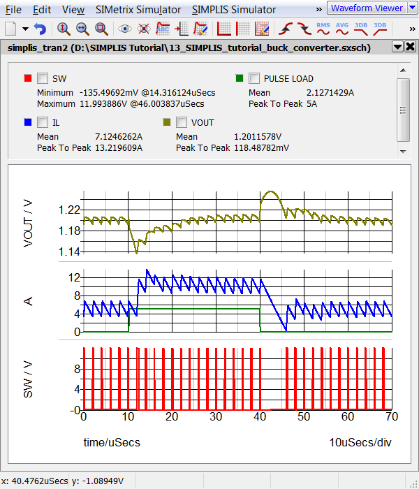
The schematic at this point is a complete hierarchical design. Although only one hierarchical block is used, the concepts in this chapter can be used to create larger and more complex hierarchical models.
The electrical model for the synchronous buck converter is electrically unchanged by adding hierarchy. Moving the compensator into a hierarchical block allows that block to:
- Be used in other controllers which need a 3-pole/2-zero compensator.
- Replaced with a different compensator, using an alternative control approach. The symbol used in the hierarchical block can be saved to another compensator block, allowing drop-in replacement of the compensator block on the parent schematic.
- Parameterized with the values defined in the parent schematic. For example, the poles and zeros could be passed into the compensator from the synchronous buck converter schematic. Parameterization is described in the Module 5 - Parameterization topic.