SIMPLIS MOSFET Options
The default test conditions for the Extract MOSFET Parameters dialog can be set from the
menu . Three advanced options are hidden by
default until you click the Show Advanced Options button.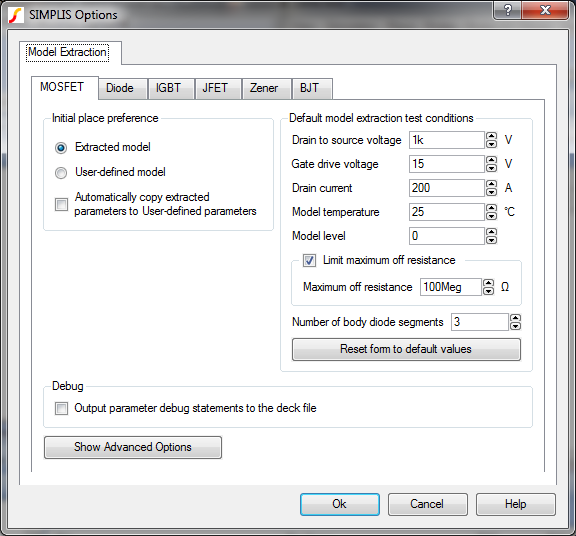
| Test Condition | Default Value | Units | Description |
| Drain to source voltage | 1k | V | The peak off-state voltage seen by this device. Used to extract capacitance for model levels which include parasitic capacitance. Breakdown is not modeled. |
| Gate drive voltage | 15 | V | Gate to source voltage to extract RDS(on). |
| Drain Current | 200 | A | Peak drain current to extract the RDS(on) and forward gain of the MOSFET. |
| Model temperature | 25 | °C | Temperature used for all extraction simulations. |
| Model level | 0 | Model complexity. For information on choosing the model level, see MOSFET Model Levels. | |
| Limit maximum off resistance | Checked | none | Limits the off resistance for the MOSFET. For some SPICE models, this will produce a SIMPLIS model which runs faster. |
| Maximum off resistance | 100Meg | W | The maximum off resistance of the MOSFET switch. This value is used only if "Limit maximum off resistance" is checked. |
| Option | Default Value | Description |
| Initial Place Preference | Extracted | Indicates which model type (Extracted or User-defined) is selected when you place the device on the schematic. |
| Automatically copy extracted parameters to User-defined parameters | Checked | If checked the extracted
parameters overwrite the user-defined parameters each time a model is
extracted. If unchecked, the user-defined parameters are never overwritten. |
| Number of body diode segments | 3 | Sets the number of segments for
the Body diode extraction algorithm. If you select 2, the algorithm models on and off resistance. If you select 3, the algorithm models a transition resistance in between the on and off segments. |
| Debug | ||
| Output parameter ... | Unchecked | If checked, the debug statements
are automatically written to the deck file. The Command shell menu opens the .deck file for editing. An example set of debug statements can be found in the Deck-Level Debug section. |
| Advanced options | Hidden | Click this button to view or
change the advanced options. For more information, see Advanced Options. |
Deck-Level Debug
If you check "Output parameter debug statements to the deck file," each MOSFET in the design has a debug report inserted in the .deck file when you run a simulation. This debug report displays the calculated values for each major parameter in a formatted table. You can edit the .deck file with the Command shell menu . A sample debug report is shown below:
***SIMPLIS DEBUG EXTRACTED MOS START********************************************
***                                                                          ***
*** Device with REF : Q1                                                     ***
***                                                                          ***
*** Extracted from SPICE model: IRF530                                       ***
***                                                                          ***
********************************************************************************
*
* Model Extraction Parameters
*
* VD_PEAK        : 900
* ID_PEAK        : 28
* VGSON          : 15
* TEMP           : 25
* LEVEL          : 0
* POL            : 1
* LIMIT_MAX_ROFF : 1
* MAX_ROFF       : 100Meg
*
*
* Conduction Parameters
*
* RDSON      : 125.171m
* ROFF       : 100Meg
*
* Forward Gain Parameters
*
* VT0        : 4.98562
* HYSTWD     : 498.562m
*
* Body Diode Parameters
*
* BD_NSEG      : 4
* R BODY SEG#1 : 1
* R BODY SEG#2 : infinite
* R BODY SEG#3 : 35.7196m
* R BODY SEG#4 : 15.9721m
*
* Body Diode V-I Conduction Points
*
* VD0        : -10.001k
* IBD0       : -1
* VD1        : -10k
* IBD1       : 0
* VD2        : 680.304m
* IBD2       : 0
* VD3        : 816.14m
* IBD3       : 3.80284
* VD4        : 1.20262
* IBD4       : 28
*
* Gate Resistance
*
* RG         : 973.603m
*
* Gate - Source Capacitance Parameters
*
* CGS        : 616.999p
*
* Drain - Gate Capacitance Parameters
*
* CDG SEG#1  : 173.8p
* CDG SEG#2  : 41.7796p
* CDG SEG#3  : 33.7874p
* CDG SEG#4  : 31.6724p
*
* Drain - Gate Charge V-Q Points
*
* CDG_NSEG   : 4
* VCDG0      : 0
* QCDG0      : 0
* VCDG1      : 19.2895
* QCDG1      : 3.35252n
* VCDG2      : 214.212
* QCDG2      : 11.4963n
* VCDG3      : 360
* QCDG3      : 16.4221n
* VCDG4      : 900
* QCDG4      : 33.5252n
*
*
* Drain - Source Capacitance Parameters
*
* CDS SEG#1  : 99.1877p
* CDS SEG#2  : 31.3306p
* CDS SEG#3  : 14.3872p
* CDS SEG#4  : 9.5245p
*
* Drain - Source Charge V-Q Points
*
* CDS_NSEG   : 4
* VCDS0      : 0
* QCDS0      : 0
* VCDS1      : 13.7018
* QCDS1      : 1.35905n
* VCDS2      : 137.995
* QCDS2      : 5.25323n
* VCDS3      : 360
* QCDS3      : 8.44727n
* VCDS4      : 900
* QCDS4      : 13.5905n
*
********************************************************************************
***                                                                          ***
*** Device with REF : Q1                                                     ***
***                                                                          ***
*** Extracted from SPICE model: IRF530                                       ***
***                                                                          ***
***SIMPLIS DEBUG EXTRACTED MOS END**********************************************